- 您現(xiàn)在的位置:買賣IC網(wǎng) > PDF目錄385568 > MC56F8345VFG60 (MOTOROLA INC) 56F8345 16-bit Hybrid Controller PDF資料下載
參數(shù)資料
| 型號(hào): | MC56F8345VFG60 |
| 廠商: | MOTOROLA INC |
| 元件分類: | 數(shù)字信號(hào)處理 |
| 英文描述: | 56F8345 16-bit Hybrid Controller |
| 中文描述: | 0-BIT, 240 MHz, OTHER DSP, PQFP128 |
| 封裝: | 14 X 20 MM, 0.50 MM PITCH, 1.40 MM HEIGHT, PLASTIC, LQFP-128 |
| 文件頁數(shù): | 18/148頁 |
| 文件大?。?/td> | 1420K |
| 代理商: | MC56F8345VFG60 |
第1頁第2頁第3頁第4頁第5頁第6頁第7頁第8頁第9頁第10頁第11頁第12頁第13頁第14頁第15頁第16頁第17頁當(dāng)前第18頁第19頁第20頁第21頁第22頁第23頁第24頁第25頁第26頁第27頁第28頁第29頁第30頁第31頁第32頁第33頁第34頁第35頁第36頁第37頁第38頁第39頁第40頁第41頁第42頁第43頁第44頁第45頁第46頁第47頁第48頁第49頁第50頁第51頁第52頁第53頁第54頁第55頁第56頁第57頁第58頁第59頁第60頁第61頁第62頁第63頁第64頁第65頁第66頁第67頁第68頁第69頁第70頁第71頁第72頁第73頁第74頁第75頁第76頁第77頁第78頁第79頁第80頁第81頁第82頁第83頁第84頁第85頁第86頁第87頁第88頁第89頁第90頁第91頁第92頁第93頁第94頁第95頁第96頁第97頁第98頁第99頁第100頁第101頁第102頁第103頁第104頁第105頁第106頁第107頁第108頁第109頁第110頁第111頁第112頁第113頁第114頁第115頁第116頁第117頁第118頁第119頁第120頁第121頁第122頁第123頁第124頁第125頁第126頁第127頁第128頁第129頁第130頁第131頁第132頁第133頁第134頁第135頁第136頁第137頁第138頁第139頁第140頁第141頁第142頁第143頁第144頁第145頁第146頁第147頁第148頁
18
56F8345 Technical Data
Preliminary
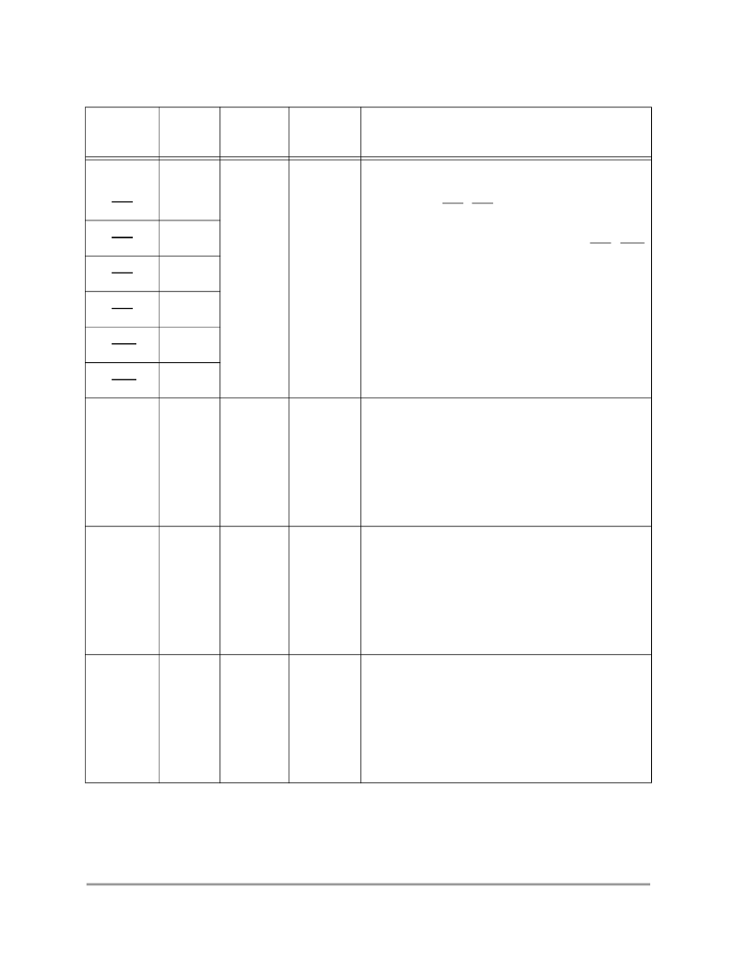
GPIOD0
(CS2)
42
Input/
Output
Output
Input
Input
Port D GPIO
— These six GPIO pins can be individually
programmed as input or output pins.
Chip Select
— CS2 - CS7 may be programmed within the
EMI module to act as chip selects for specific areas of the
external memory map. Depending upon the state of the
DRV bit in the EMI bus control register (BCR), CS2 - CS7
are tri-stated when the external bus is inactive.
After reset, these pins are configured as GPIO.
To deactivate the internal pull-up resistor, clear the
appropriate GPIO bit in the GPIOD_PUR register.
Example: GPIOD0, clear bit 0 in the GPIOD_PUR
register.
GPIOD1
(CS3)
43
GPIOD2
(CS4)
44
GPIOD3
(CS5)
45
GPIOD4
(CS6)
46
GPIOD5
(CS7)
47
TXD0
(GPIOE0)
7
Output
Input/
Output
Tri-stated
Input
Transmit Data
— SCI0 transmit data output
Port E GPIO
— This GPIO pin can be individually
programmed as an input or output pin.
After reset, the default state is SCI output.
To deactivate the internal pull-up resistor, clear bit 0 in the
GPIOE_PUR register.
RXD0
(GPIOE1)
8
Input
Input/
Output
Input
Input
Receive Data
— SCI0 receive data input
Port E GPIO
— This GPIO pin can be individually
programmed as an input or output pin.
After reset, the default state is SCI output.
To deactivate the internal pull-up resistor, clear bit 1 in the
GPIOE_PUR register.
TXD1
(GPIOD6)
40
Output
Input/
Output
Tri-stated
Input
Transmit Data
— SCI1 transmit data output
Port D GPIO
— This GPIO pin can be individually
programmed as an input or output pin.
After reset, the default state is SCI output.
To deactivate the internal pull-up resistor, clear bit 6 in the
GPIOD_PUR register.
Table 2-2 56F8345 Signal and Package Information for the 128-Pin LQFP
Signal
Name
Pin No.
Type
State
During
Reset
Signal Description
F
Freescale Semiconductor, Inc.
For More Information On This Product,
Go to: www.freescale.com
n
.
相關(guān)PDF資料 |
PDF描述 |
|---|---|
| MC68HC912B32FU8 | Evaluation Board |
| MC74AC14 | Hex Inverter Schmitt Trigger(六反相施密特觸發(fā)器) |
| MC74AC273 | Octal D Flip Flop(八D觸發(fā)器) |
| MC74AC32 | Quad 2(四2輸入或門) |
| MC74AC373 | Octal Transparent Latch with 3 State Outputs(八D鎖存器(三態(tài)輸出)) |
相關(guān)代理商/技術(shù)參數(shù) |
參數(shù)描述 |
|---|---|
| MC56F8345VFGE | 功能描述:數(shù)字信號(hào)處理器和控制器 - DSP, DSC 16 BIT HYBRID CONTROLLER RoHS:否 制造商:Microchip Technology 核心:dsPIC 數(shù)據(jù)總線寬度:16 bit 程序存儲(chǔ)器大小:16 KB 數(shù)據(jù) RAM 大小:2 KB 最大時(shí)鐘頻率:40 MHz 可編程輸入/輸出端數(shù)量:35 定時(shí)器數(shù)量:3 設(shè)備每秒兆指令數(shù):50 MIPs 工作電源電壓:3.3 V 最大工作溫度:+ 85 C 封裝 / 箱體:TQFP-44 安裝風(fēng)格:SMD/SMT |
| MC56F8346 | 制造商:FREESCALE 制造商全稱:Freescale Semiconductor, Inc 功能描述:16-bit Digital Signal Controllers |
| MC56F8346EVM | 制造商:Freescale Semiconductor 功能描述:Tools Development kit Kit Contents:Inst |
| MC56F8346MFV60 | 功能描述:數(shù)字信號(hào)處理器和控制器 - DSP, DSC 60MHz 60MIPS RoHS:否 制造商:Microchip Technology 核心:dsPIC 數(shù)據(jù)總線寬度:16 bit 程序存儲(chǔ)器大小:16 KB 數(shù)據(jù) RAM 大小:2 KB 最大時(shí)鐘頻率:40 MHz 可編程輸入/輸出端數(shù)量:35 定時(shí)器數(shù)量:3 設(shè)備每秒兆指令數(shù):50 MIPs 工作電源電壓:3.3 V 最大工作溫度:+ 85 C 封裝 / 箱體:TQFP-44 安裝風(fēng)格:SMD/SMT |
| MC56F8346MFVE | 功能描述:數(shù)字信號(hào)處理器和控制器 - DSP, DSC 16 BIT HYBRID CONTROLLER RoHS:否 制造商:Microchip Technology 核心:dsPIC 數(shù)據(jù)總線寬度:16 bit 程序存儲(chǔ)器大小:16 KB 數(shù)據(jù) RAM 大小:2 KB 最大時(shí)鐘頻率:40 MHz 可編程輸入/輸出端數(shù)量:35 定時(shí)器數(shù)量:3 設(shè)備每秒兆指令數(shù):50 MIPs 工作電源電壓:3.3 V 最大工作溫度:+ 85 C 封裝 / 箱體:TQFP-44 安裝風(fēng)格:SMD/SMT |
發(fā)布緊急采購(gòu),3分鐘左右您將得到回復(fù)。