- 您現(xiàn)在的位置:買賣IC網(wǎng) > PDF目錄384708 > MAX8632ETI (Maxim Integrated Products, Inc.) Quadruple 2-Input Positive-NAND Gates With Open-Drain Outputs 14-CDIP -55 to 125 PDF資料下載
參數(shù)資料
| 型號: | MAX8632ETI |
| 廠商: | Maxim Integrated Products, Inc. |
| 英文描述: | Quadruple 2-Input Positive-NAND Gates With Open-Drain Outputs 14-CDIP -55 to 125 |
| 中文描述: | 集成的DDR電源適用于臺式機,筆記本電腦解決方案和圖形卡 |
| 文件頁數(shù): | 13/29頁 |
| 文件大?。?/td> | 512K |
| 代理商: | MAX8632ETI |
第1頁第2頁第3頁第4頁第5頁第6頁第7頁第8頁第9頁第10頁第11頁第12頁當前第13頁第14頁第15頁第16頁第17頁第18頁第19頁第20頁第21頁第22頁第23頁第24頁第25頁第26頁第27頁第28頁第29頁
The on-time one-shot has good accuracy at the operat-
ing points specified in the
Electrical Characteristics
table (approximately ±12.5% at 600kHz and 450kHz,
and ±10% at 200kHz and 300kHz). On-times at operat-
ing points far removed from the conditions specified in
the
Electrical Characteristics
table can vary over a
wider range. For example, the 600kHz setting typically
runs approximately 10% slower with inputs much
greater than 5V due to the very short on-times required.
The constant on-time translates only roughly to a con-
stant switching frequency. The on-times guaranteed in
the
Electrical Characteristics
table are influenced by
resistive losses and by switching delays in the high-
side MOSFET. Resistive losses, which include the
inductor, both MOSFETs, the output capacitor’s ESR,
and any PC board copper losses in the output and
ground, tend to raise the switching frequency as the
load increases. The dead-time effect increases the
effective on-time, reducing the switching frequency as
one or both dead times are added to the effective on-
time. The dead time occurs only in PWM mode (
SKIP
=
V
DD
) and during dynamic output-voltage transitions
when the inductor current reverses at light or negative
load currents. With reversed inductor current, the induc-
tor’s EMF causes LX to go high earlier than normal,
extending the on-time by a period equal to the DH-rising
dead time. For loads above the critical conduction point,
where the dead-time effect is no longer a factor, the
actual switching frequency is:
where V
DROP1
is the sum of the parasitic voltage drops
in the inductor discharge path, including the synchro-
nous rectifier, the inductor, and any PC board resis-
tances; V
DROP2
is the sum of the resistances in the
charging path, including the high-side switch (Q1 in the
Typical Applications Circuit of Figure 8), the inductor,
and any PC board resistances, and t
ON
is the one-shot
on-time (see the
On-Time One-Shot (TON)
section.
Automatic Pulse-Skipping Mode
(
SKIP
= GND)
In skip mode (
SKIP
= GND), an inherent automatic
switchover to PFM takes place at light loads (Figure 2).
This switchover is affected by a comparator that trun-
cates the low-side switch on-time at the inductor cur-
rent’s zero crossing. The zero-crossing comparator
differentially senses the inductor current across the
synchronous-rectifier MOSFET (Q2 in the Typical
Applications Circuit of Figure 8). Once V
PGND
- V
LX
drops below 5% of the current-limit threshold (2.5mV
for the default 50mV current-limit threshold), the com-
parator forces DL low (Figure 1). This mechanism caus-
es the threshold between pulse-skipping PFM and
nonskipping PWM operation to coincide with the
boundary between continuous and discontinuous
inductor-current operation (also known as the critical
conduction point). The load-current level at which
PFM/PWM crossover occurs, I
LOAD(SKIP)
, is equal to
half the peak-to-peak ripple current, which is a function
of the inductor value (Figure 2). This threshold is rela-
tively constant, with only a minor dependence on the
input voltage (V
IN
):
where K is the on-time scale factor (see Table 1). For
example, in the Typical Applications Circuit of Figure 8
(K = 1.7μs, V
OUT
= 2.5V, V
IN
= 12V, and L = 1μH), the
pulse-skipping switchover occurs at:
The crossover point occurs at an even lower value if a
swinging (soft-saturation) inductor is used. The switching
waveforms can appear noisy and asynchronous when
light loading causes pulse-skipping operation, but this is
a normal operating condition that results in high light-
load efficiency. Trade-offs in PFM noise vs. light-load
efficiency are made by varying the inductor value.
Generally, low inductor values produce a broader effi-
ciency vs. load curve, while higher values result in higher
full-load efficiency (assuming that the coil resistance
2 5
.
1
μ
2
12
2
V
12
1 68
.
1 7
×
V
s
H
V
A
=
μ
- .5V
I
V
K
L
V
V
V
LOAD SKIP
OUT
IN
OUT
IN
(
)
×
=
2
-
f
V
V
V
t
V
SW
OUT
DROP
DROP
ON
IN
+
=
+
)
1
2
M
Integrated DDR Power-Supply Solution for
Desktops, Notebooks, and Graphic Cards
______________________________________________________________________________________
13
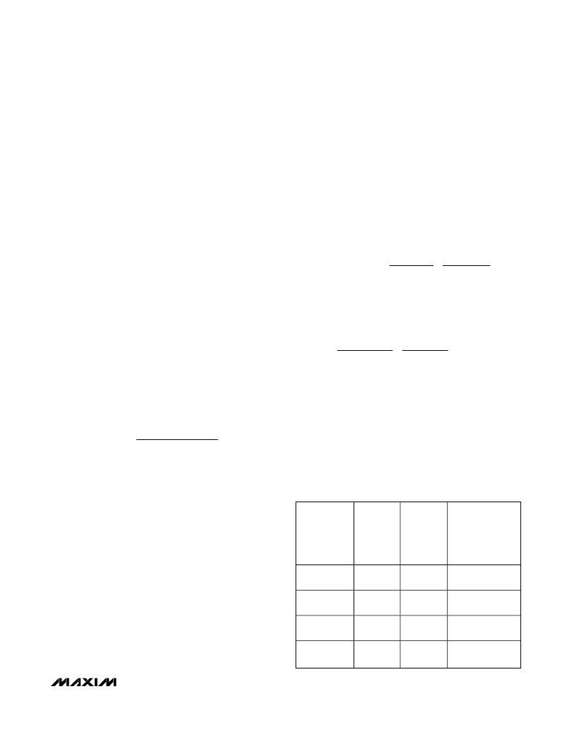
Table 1. Approximate K-Factor Errors
TON SETTING
TYPICAL
K-FACTOR
(μs)
K-FACTOR
ERROR
(%)
MINIMUM V
IN
AT
V
OUT
= 2.5V
(h = 1.5; SEE THE
DROPOUT
PERFORMANCE
(BUCK)
SECTION)
200
(TON = AV
DD
)
5.0
±
10
3.15
300
(TON = open)
3.3
±
10
3.47
450
(TON = REF)
2.2
±
12.5
4.13
600
(TON = GND)
1.7
±
12.5
5.61
相關(guān)PDF資料 |
PDF描述 |
|---|---|
| MAX8632 | Quadruple 2-Input Positive-NAND Gates With Open-Drain Outputs 20-LCCC -55 to 125 |
| MAX863EEE | Dual, High-Efficiency, PFM, Step-Up DC-DC Controller |
| MAX864 | Dual-Output Charge Pump with Shutdown |
| MAX864EEE | Dual-Output Charge Pump with Shutdown |
| MAX865 | Compact, Dual-Output Charge Pump |
相關(guān)代理商/技術(shù)參數(shù) |
參數(shù)描述 |
|---|---|
| MAX8632ETI+ | 功能描述:PMIC 解決方案 DDR Power-Supply Solution RoHS:否 制造商:Texas Instruments 安裝風(fēng)格:SMD/SMT 封裝 / 箱體:QFN-24 封裝:Reel |
| MAX8632ETI+T | 功能描述:PMIC 解決方案 DDR Power-Supply Solution RoHS:否 制造商:Texas Instruments 安裝風(fēng)格:SMD/SMT 封裝 / 箱體:QFN-24 封裝:Reel |
| MAX8632ETI+TGD2 | 制造商:Rochester Electronics LLC 功能描述: 制造商:Maxim Integrated Products 功能描述: |
| MAX8632EVKIT | 功能描述:電源管理IC開發(fā)工具 RoHS:否 制造商:Maxim Integrated 產(chǎn)品:Evaluation Kits 類型:Battery Management 工具用于評估:MAX17710GB 輸入電壓: 輸出電壓:1.8 V |
| MAX8633ELA+ | 制造商:Maxim Integrated Products 功能描述: |
發(fā)布緊急采購,3分鐘左右您將得到回復(fù)。