- 您現(xiàn)在的位置:買賣IC網(wǎng) > PDF目錄384688 > MAX5945CAX (MAXIM INTEGRATED PRODUCTS INC) Quad Network Power Controller for Power-Over-LAN PDF資料下載
參數(shù)資料
| 型號: | MAX5945CAX |
| 廠商: | MAXIM INTEGRATED PRODUCTS INC |
| 元件分類: | 電源管理 |
| 英文描述: | Quad Network Power Controller for Power-Over-LAN |
| 中文描述: | 4-CHANNEL POWER SUPPLY MANAGEMENT CKT, PDSO36 |
| 封裝: | 0.80 MM PICTH, SSOP-36 |
| 文件頁數(shù): | 2/44頁 |
| 文件大小: | 572K |
| 代理商: | MAX5945CAX |
第1頁當前第2頁第3頁第4頁第5頁第6頁第7頁第8頁第9頁第10頁第11頁第12頁第13頁第14頁第15頁第16頁第17頁第18頁第19頁第20頁第21頁第22頁第23頁第24頁第25頁第26頁第27頁第28頁第29頁第30頁第31頁第32頁第33頁第34頁第35頁第36頁第37頁第38頁第39頁第40頁第41頁第42頁第43頁第44頁
M
Quad Network Power Controller
for Power-Over-LAN
2
_______________________________________________________________________________________
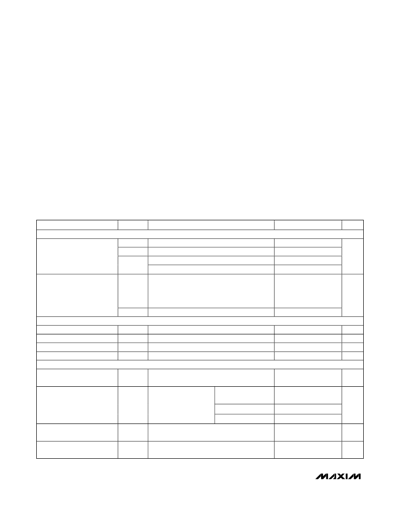
ABSOLUTE MAXIMUM RATINGS
(Voltages referenced to V
EE
, unless otherwise noted.)
AGND, DGND, DET_, V
DD
,
RESET
, A3, A2, A1, A0,
SHD_
,
OSC_IN, SCL, SDAIN, OUT_ and AUTO............-0.3V to +80V
GATE_ (internally clamped, Note 1)....................-0.3V to +11.4V
SENSE_ ..................................................................-0.3V to +24V
V
DD
,
RESET
, A3, A2, A1, A0,
SHD_
, OSC_IN, SCL, SDAIN and
AUTO to DGND....................................................-0.3V to +7V
INT
and SDAOUT to DGND....................................-0.3V to +12V
Maximum Current into
INT
, SDAOUT, DET_.......................80mA
Stresses beyond those listed under “Absolute Maximum Ratings” may cause permanent damage to the device. These are stress ratings only, and functional
operation of the device at these or any other conditions beyond those indicated in the operational sections of the specifications is not implied. Exposure to
absolute maximum rating conditions for extended periods may affect device reliability.
ELECTRICAL CHARACTERISTICS
(AGND = +32V to +60V, V
EE
= 0V, V
DD
to DGND = +3.3V, all voltages are referenced to V
EE
, unless otherwise noted. Typical
values are at AGND = +48V, DGND = +48V, V
DD
= (DGND + 3.3V), T
A
= +25°C. Currents are positive when entering the pin and
negative otherwise.)
Maximum Power Dissipation
36-Pin SSOP (derate 11.4mW/°C above +70°C) .........941mW
Operating Temperature Ranges:
MAX5945EAX ..................................................-40°C to +85°C
MAX5945CAX .....................................................0°C to +70°C
Storage Temperature Range.............................-65°C to +150°C
Junction Temperature......................................................+150°C
Lead Temperature (soldering, 10s).................................+300°C
PARAMETER
SYMBOL
CONDITIONS
MIN
TYP
MAX
UNITS
POWER SUPPLIES
V
AGND
V
DGND
V
AGND
- V
EE
32
0
1.71
3.0
60
60
5.50
5.5
V
DD
to V
DGND
,
V
DGND
= V
AGND
V
DD
to V
DGND
,
V
DGND
= V
EE
Operating Voltage Range
V
DD
V
I
EE
OUT_ = V
EE
, SENSE_ = V
EE
, DET_ = AGND,
all logic inputs open, SCL = SDAIN = V
DD
,
INT
and SDAOUT open; measured at AGND
in power mode after GATE_ pullup
4.2
6.8
Supply Currents
I
DIG
All logic inputs high, measured at V
DD
2.7
5.6
mA
GATE DRIVER AND CLAMPING
GATE_ Pullup Current
Weak GATE_ Pulldown Current
Maximum Pulldown Current
External Gate Drive
CURRENT LIMIT
I
PU
I
PDW
I
PDS
V
GS
Power mode, gate drive on, V
GATE
= V
EE
(Note
2)
SHD_
= DGND, V
GATE_
= V
EE
+ 5V
V
SENSE
= 1V, V
GATE_
= V
EE
+ 2V
V
GATE
- V
EE
, power mode, gate drive on
-40
30
-50
40
100
10
-60
50
μA
μA
mA
V
9
11
Current-Limit Clamp Voltage
V
SU_LIM
Maximum V
SENSE_
allowed during current limit,
V
OUT_
= V
EE
(Note 3)
202
212
220
mV
Default, class 0,
class 3, class 4
178.5
196
Class 1
49
61
Overcurrent Threshold After
Startup
V
FLT_LIM
Overcurrent V
SENSE_
threshold
allowed for
t
≤
t
FAULT
after startup;
V
OUT_
= V
EE
Class 2
90
104
mV
Foldback Initial OUT_ Voltage
V
FLBK_ST
V
OUT_
- V
EE
, above which the current-limit trip
voltage starts folding back
30
V
Foldback Final OUT_ Voltage
V
FLBK_END
V
OUT_
- V
EE
, above which the current-limit trip
voltage reaches V
TH_FB
50
V
Note 1:
GATE_ is internally clamped to 11.4V above V
EE
. Driving GATE_ higher than 11.4V above V
EE
may damage the device.
相關(guān)PDF資料 |
PDF描述 |
|---|---|
| MAX5945EAX | Quad Network Power Controller for Power-Over-LAN |
| MAX5948 | AND-OR-invert Gates 14-CFP -55 to 125 |
| MAX5948A | -48V Hot-Swap Controllers with External RSENSE |
| MAX5948AESA | -48V Hot-Swap Controllers with External RSENSE |
| MAX5948B | 4-2-3-2 Input AND-OR-invert Gates 14-CDIP -55 to 125 |
相關(guān)代理商/技術(shù)參數(shù) |
參數(shù)描述 |
|---|---|
| MAX5945CAX+ | 功能描述:熱插拔功率分布 IEEE 802.3af Quad Net Pwr Controller RoHS:否 制造商:Texas Instruments 產(chǎn)品:Controllers & Switches 電流限制: 電源電壓-最大:7 V 電源電壓-最小:- 0.3 V 工作溫度范圍: 功率耗散: 安裝風(fēng)格:SMD/SMT 封裝 / 箱體:MSOP-8 封裝:Tube |
| MAX5945CAX+T | 功能描述:熱插拔功率分布 IEEE 802.3af Quad Net Pwr Controller RoHS:否 制造商:Texas Instruments 產(chǎn)品:Controllers & Switches 電流限制: 電源電壓-最大:7 V 電源電壓-最小:- 0.3 V 工作溫度范圍: 功率耗散: 安裝風(fēng)格:SMD/SMT 封裝 / 箱體:MSOP-8 封裝:Tube |
| MAX5945CAX-T | 功能描述:熱插拔功率分布 RoHS:否 制造商:Texas Instruments 產(chǎn)品:Controllers & Switches 電流限制: 電源電壓-最大:7 V 電源電壓-最小:- 0.3 V 工作溫度范圍: 功率耗散: 安裝風(fēng)格:SMD/SMT 封裝 / 箱體:MSOP-8 封裝:Tube |
| MAX5945EAX | 功能描述:熱插拔功率分布 RoHS:否 制造商:Texas Instruments 產(chǎn)品:Controllers & Switches 電流限制: 電源電壓-最大:7 V 電源電壓-最小:- 0.3 V 工作溫度范圍: 功率耗散: 安裝風(fēng)格:SMD/SMT 封裝 / 箱體:MSOP-8 封裝:Tube |
| MAX5945EAX+ | 功能描述:熱插拔功率分布 IEEE 802.3af Quad Net Pwr Controller RoHS:否 制造商:Texas Instruments 產(chǎn)品:Controllers & Switches 電流限制: 電源電壓-最大:7 V 電源電壓-最小:- 0.3 V 工作溫度范圍: 功率耗散: 安裝風(fēng)格:SMD/SMT 封裝 / 箱體:MSOP-8 封裝:Tube |
發(fā)布緊急采購,3分鐘左右您將得到回復(fù)。