- 您現(xiàn)在的位置:買賣IC網(wǎng) > PDF目錄384688 > MAX5945CAX (MAXIM INTEGRATED PRODUCTS INC) Quad Network Power Controller for Power-Over-LAN PDF資料下載
參數(shù)資料
| 型號(hào): | MAX5945CAX |
| 廠商: | MAXIM INTEGRATED PRODUCTS INC |
| 元件分類: | 電源管理 |
| 英文描述: | Quad Network Power Controller for Power-Over-LAN |
| 中文描述: | 4-CHANNEL POWER SUPPLY MANAGEMENT CKT, PDSO36 |
| 封裝: | 0.80 MM PICTH, SSOP-36 |
| 文件頁(yè)數(shù): | 11/44頁(yè) |
| 文件大?。?/td> | 572K |
| 代理商: | MAX5945CAX |
第1頁(yè)第2頁(yè)第3頁(yè)第4頁(yè)第5頁(yè)第6頁(yè)第7頁(yè)第8頁(yè)第9頁(yè)第10頁(yè)當(dāng)前第11頁(yè)第12頁(yè)第13頁(yè)第14頁(yè)第15頁(yè)第16頁(yè)第17頁(yè)第18頁(yè)第19頁(yè)第20頁(yè)第21頁(yè)第22頁(yè)第23頁(yè)第24頁(yè)第25頁(yè)第26頁(yè)第27頁(yè)第28頁(yè)第29頁(yè)第30頁(yè)第31頁(yè)第32頁(yè)第33頁(yè)第34頁(yè)第35頁(yè)第36頁(yè)第37頁(yè)第38頁(yè)第39頁(yè)第40頁(yè)第41頁(yè)第42頁(yè)第43頁(yè)第44頁(yè)
M
Quad Network Power Controller
for Power-Over-LAN
______________________________________________________________________________________
11
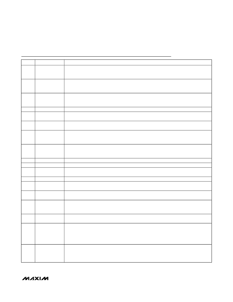
PIN
NAME
FUNCTION
1
RESET
Hardware Reset. Pull
RESET
low for at least 300μs to reset the device. All internal registers reset to
their default value. The address (A0–A3), and AUTO and MIDSPAN input logic levels latch on during
low-to-high transition of
RESET
. Internally pulled up to V
DD
with 50k
resistor.
MIDSPAN Mode Input. An internal 50k
pulldown resistor to DGND sets the default mode to endpoint
PSE operation (power-over-signal pairs). Pull MIDSPAN TO V
DIG
to set MIDSPAN operation. The
MIDSPAN value latches after the IC is powered up or reset (see the
PD Detection
section).
2
MIDSPAN
3
INT
Open-Drain Interrupt Output.
INT
goes low whenever a fault condition exists. Reset the fault condition
using software or by pulling
RESET
low (see the
Interrupt
section of the
Detailed Description
for more
information about interrupt management).
Serial Interface Clock Line
Serial Output Data Line. Connect the data line optocoupler input to SDAOUT (see the
Typical
Application Circuit
). Connect SDAOUT to SDAIN if using a 2-wire I
2
C-compatible system.
Serial Interface Input Data Line. Connect the data line optocoupler output SDAIN (see the
Typical
Application Circuit
). Connect SDAIN to SDAOUT if using a 2-wire wire I
2
C-compatible system.
Address Bits. A3, A2, A1, and A0 form the lower part of the device’s address. Address inputs default
high with an internal 50k
pullup resistor to V
DD
. The address values latch when V
DD
or V
EE
ramps
up and exceeds its UVLO threshold or after a reset. The 3 MSB bits of the address are set to 010.
4
SCL
5
SDAOUT
6
SDAIN
7–10
A3, A2, A1, A0
11–14
DET1, DET2,
DET3, DET4
Detection and Classification Voltage Outputs. Use DET1 to set the detection and classification probe
voltages on port 1. Use DET1 for the AC voltage sensing of port 1 when using the AC disconnect
scheme (see the
Typical Application Circuit
).
Connect to Digital Ground
Positive Digital Supply. Connect to digital supply (referenced to DGND).
Port Shutdown Inputs. Pull
SHD_
low to turn off the external FET on port_. Internally pulled up to V
DD
with a 50k
resistor.
Analog Ground. Connect to the high-side analog supply.
MOSFET Source Current-Sense Negative Inputs. Connect to the source of the power MOSFET and
connect a current-sense resistor between SENSE_ and V
EE
(see the
Typical Application Circuit
).
Port_ MOSFET Gate Drivers. Connect GATE_ to the gate of the external FET (see the
Typical
Application Circuit
).
MOSFET Drain-Output Voltage Senses. Connect OUT_ to the power MOSFET drain through a resistor
(100
to 100k
). The low leakage at OUT_ limits the drop across the resistor to less than 100mV
(see the
Typical Application Circuit
).
15
16
DGND
V
DD
17–20
SHD1
,
SHD2
,
SHD3
,
SHD4
AGND
SENSE4, SENSE3,
SENSE2, SENSE1
GATE4, GATE3,
GATE2, GATE1
21
22, 25,
29, 32
23, 26,
30, 33
24, 27,
31, 34
OUT4, OUT3,
OUT2, OUT1
28
V
EE
Low-Side Analog Supply Input. Connect the low-side analog supply to V
EE
(-48V). Bypass with a 1μF
capacitor between AGND and V
EE
.
AUTO or SHUTDOWN Mode Input. Force high to enter AUTO mode after a reset or power-up. Drive
low to put the MAX5945 into SHUTDOWN mode. In SHUTDOWN mode, software controls the
operational modes of the MAX5945. A 50k
internal pulldown resistor defaults AUTO low. AUTO
latches when V
DD
or V
EE
ramps up and exceeds its UVLO threshold or when the device resets.
Software commands can take the MAX5945 out of AUTO while AUTO is high.
Oscillator Input. AC-disconnect detection function uses OSC_IN. Connect a 100Hz ±10%, 2V
P-P
±5%, +1.2V offset sine wave to OSC_IN. If the oscillator positive peak falls below the OSC_FAIL
threshold of 2V, the ports that have the AC function enabled shut down and are not allowed to power
up. When not using the AC-disconnect detection function, leave OSC_IN unconnected.
35
AUTO
36
OSC_IN
Pin Description
相關(guān)PDF資料 |
PDF描述 |
|---|---|
| MAX5945EAX | Quad Network Power Controller for Power-Over-LAN |
| MAX5948 | AND-OR-invert Gates 14-CFP -55 to 125 |
| MAX5948A | -48V Hot-Swap Controllers with External RSENSE |
| MAX5948AESA | -48V Hot-Swap Controllers with External RSENSE |
| MAX5948B | 4-2-3-2 Input AND-OR-invert Gates 14-CDIP -55 to 125 |
相關(guān)代理商/技術(shù)參數(shù) |
參數(shù)描述 |
|---|---|
| MAX5945CAX+ | 功能描述:熱插拔功率分布 IEEE 802.3af Quad Net Pwr Controller RoHS:否 制造商:Texas Instruments 產(chǎn)品:Controllers & Switches 電流限制: 電源電壓-最大:7 V 電源電壓-最小:- 0.3 V 工作溫度范圍: 功率耗散: 安裝風(fēng)格:SMD/SMT 封裝 / 箱體:MSOP-8 封裝:Tube |
| MAX5945CAX+T | 功能描述:熱插拔功率分布 IEEE 802.3af Quad Net Pwr Controller RoHS:否 制造商:Texas Instruments 產(chǎn)品:Controllers & Switches 電流限制: 電源電壓-最大:7 V 電源電壓-最小:- 0.3 V 工作溫度范圍: 功率耗散: 安裝風(fēng)格:SMD/SMT 封裝 / 箱體:MSOP-8 封裝:Tube |
| MAX5945CAX-T | 功能描述:熱插拔功率分布 RoHS:否 制造商:Texas Instruments 產(chǎn)品:Controllers & Switches 電流限制: 電源電壓-最大:7 V 電源電壓-最小:- 0.3 V 工作溫度范圍: 功率耗散: 安裝風(fēng)格:SMD/SMT 封裝 / 箱體:MSOP-8 封裝:Tube |
| MAX5945EAX | 功能描述:熱插拔功率分布 RoHS:否 制造商:Texas Instruments 產(chǎn)品:Controllers & Switches 電流限制: 電源電壓-最大:7 V 電源電壓-最小:- 0.3 V 工作溫度范圍: 功率耗散: 安裝風(fēng)格:SMD/SMT 封裝 / 箱體:MSOP-8 封裝:Tube |
| MAX5945EAX+ | 功能描述:熱插拔功率分布 IEEE 802.3af Quad Net Pwr Controller RoHS:否 制造商:Texas Instruments 產(chǎn)品:Controllers & Switches 電流限制: 電源電壓-最大:7 V 電源電壓-最小:- 0.3 V 工作溫度范圍: 功率耗散: 安裝風(fēng)格:SMD/SMT 封裝 / 箱體:MSOP-8 封裝:Tube |
發(fā)布緊急采購(gòu),3分鐘左右您將得到回復(fù)。