- 您現(xiàn)在的位置:買賣IC網(wǎng) > PDF目錄1938 > MAX3109ETJ+ (Maxim Integrated Products)SEMICONDUCTOR OTHER PDF資料下載
參數(shù)資料
| 型號(hào): | MAX3109ETJ+ |
| 廠商: | Maxim Integrated Products |
| 文件頁數(shù): | 7/66頁 |
| 文件大小: | 0K |
| 描述: | SEMICONDUCTOR OTHER |
| 標(biāo)準(zhǔn)包裝: | 60 |
| 系列: | * |
第1頁第2頁第3頁第4頁第5頁第6頁當(dāng)前第7頁第8頁第9頁第10頁第11頁第12頁第13頁第14頁第15頁第16頁第17頁第18頁第19頁第20頁第21頁第22頁第23頁第24頁第25頁第26頁第27頁第28頁第29頁第30頁第31頁第32頁第33頁第34頁第35頁第36頁第37頁第38頁第39頁第40頁第41頁第42頁第43頁第44頁第45頁第46頁第47頁第48頁第49頁第50頁第51頁第52頁第53頁第54頁第55頁第56頁第57頁第58頁第59頁第60頁第61頁第62頁第63頁第64頁第65頁第66頁
Dual Serial UART with 128-Word FIFOs
MAX3109
15
Maxim Integrated
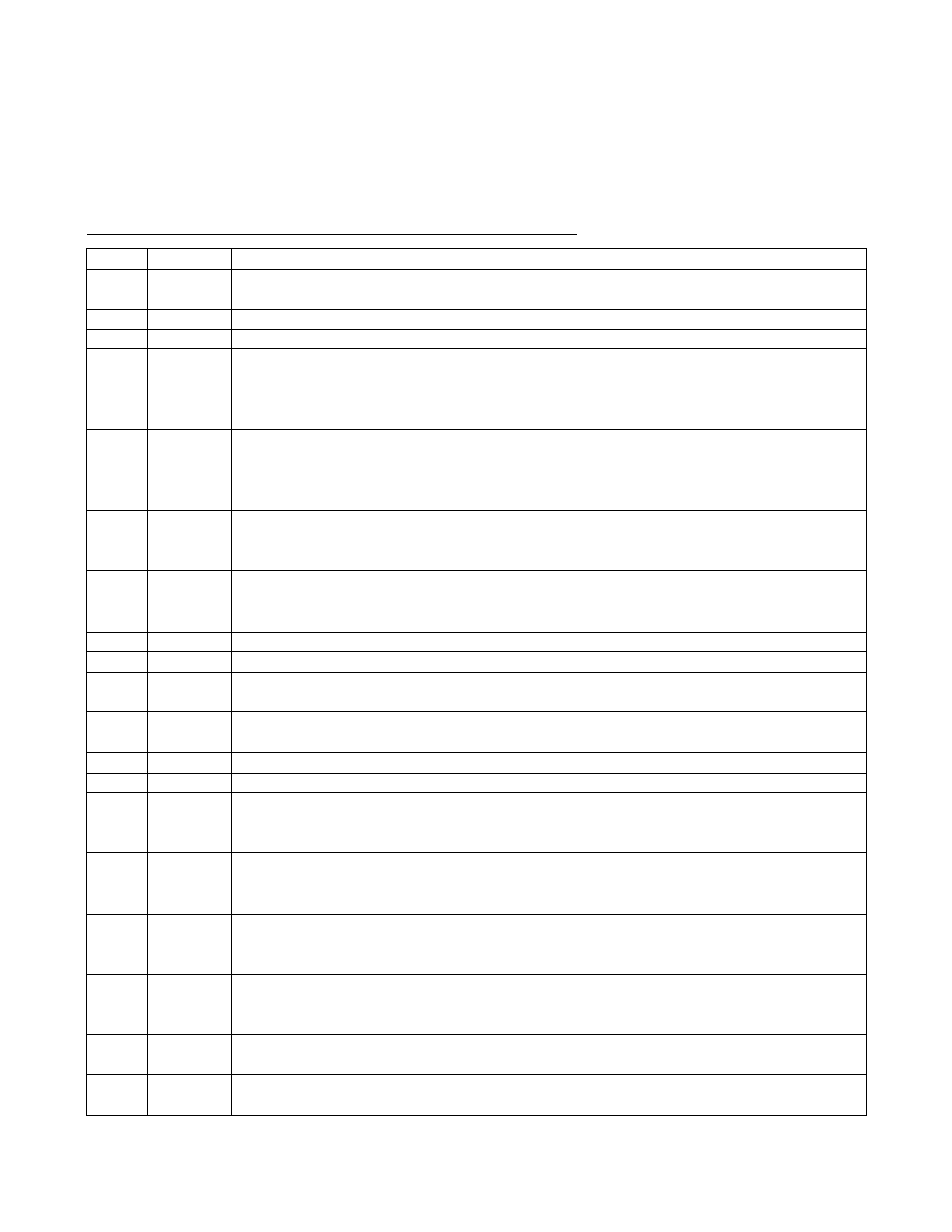
Pin Description (continued)
PIN
NAME
FUNCTION
8
VL
Digital Interface Power Supply. VL powers the internal logic-level translators for RST, IRQ, MOSI/A1, CS/A0,
SCLK/SCL, MISO/SDA, LDOEN, and SPI/I2C. Bypass VL with a 0.1FF ceramic capacitor to DGND.
9
SPI/I2C
SPI Selector Input or Active-Low I2C. Drive SPI/I2C low to enable I2C. Drive SPI/I2C high to enable SPI.
10
DGND
Digital Ground
11
GPIO0
General-Purpose Input/Output 0. GPIO0 is user-programmable as an input or output (push-pull or open
drain) or an external event-driven interrupt source. GPIO0 has a weak pulldown resistor to DGND when
configured as an input. GPIO0 is the reference clock output when bit 7 of the TxSynch register is set to
high (see the UART Clock to GPIO section for more information).
12
GPIO4
General-Purpose Input/Output 4. GPIO4 is user-programmable as an input or output (push-pull or open
drain) or an external event-driven interrupt source. GPIO4 has a weak pulldown resistor to DGND when
configured as an input. GPIO4 is the reference clock output when bit 7 of the TxSynch register is set to
high (see the UART Clock to GPIO section for more information).
13
GPIO1
General-Purpose Input/Output 1. GPIO1 is user-programmable as an input or output (push-pull or open
drain) or an external event-driven interrupt source. GPIO1 has a weak pulldown resistor to DGND when
configured as an input. GPIO1 is the TIMER output when bit 7 of the TIMER2 register is set high.
14
GPIO5
General-Purpose Input/Output 5. GPIO5 is user-programmable as an input or output (push-pull or open
drain) or an external event-driven interrupt source. GPIO5 has a weak pulldown resistor to DGND when
configured as an input. GPIO5 is the TIMER output when bit 7 of the TIMER2 register is set high.
15
CTS0
Active-Low Clear-to-Send Input for UART0. CTS0 is a flow-control status input.
16
CTS1
Active-Low Clear-to-Send Input for UART1. CTS1 is a flow-control status input.
17
TX1
Serial Transmitting Data Output for UART1. TX1 is logic-high when RST is low or when the externally
supplied V18 is not powered.
18
TX0
Serial Transmitting Data Output for UART0. TX0 is logic-high when RST is low or when the externally
supplied V18 is not powered.
19
RX0
Serial Receiving Data Input for UART0. RX0 has an internal weak pullup resistor to VEXT.
20
RX1
Serial Receiving Data Input for UART1. RX1 has an internal weak pullup resistor to VEXT.
21
RTS0
Active-Low Request-to-Send Output for UART0. RTS0 can be set high or low by programming the LCR
register. RTS0 is the UART system clock/fractional divider output when bit 7 of the CLKSource register is
set high. RTS0 is logic-high when RST is low or when the externally supplied V18 is not powered.
22
RTS1
Active-Low Request-to-Send Output for UART1. RTS1 can be set high or low by programming the LCR
register. RTS1 is the UART system clock/fractional divider output when bit 7 of the CLKSource register is
set high. RTS1 is logic-high when RST is low or when the externally supplied V18 is not powered.
23
GPIO2
General-Purpose Input/Output 2. GPIO2 is user-programmable as input or output (push-pull or open
drain) or an external event-driven interrupt source. GPIO2 has a weak pulldown resistor to DGND when
configured as an input.
24
GPIO3
General-Purpose Input/Output 3. GPIO3 is user-programmable as input or output (push-pull or open
drain) or an external event-driven interrupt source. GPIO3 has a weak pulldown resistor to DGND when
configured as an input.
25
VEXT
Transceiver Interface Power Supply. VEXT powers the internal logic-level translators for RX_, TX_, RTS_,
CTS_, and GPIO_. Bypass VEXT with a 0.1FF ceramic capacitor to DGND.
26
XIN
Crystal/Clock Input. When using an external crystal, connect one end of the crystal to XIN and the other
end to XOUT. When using an external clock source, drive XIN with the single-ended external clock.
相關(guān)PDF資料 |
PDF描述 |
|---|---|
| MAX310CPE | IC VIDEO MULTIPLEXER 8X1 16DIP |
| MAX3110EENI+G36 | IC UART SPI COMPAT 28-DIP |
| MAX3120CUA+ | IC TXRX INFRARED IRDA 8-UMAX |
| MAX3120EUA | IC TXRX 3V IRDA IR 3V 8-UMAX |
| MAX312ESE | IC SWITCH QUAD SPST 16SOIC |
相關(guān)代理商/技術(shù)參數(shù) |
參數(shù)描述 |
|---|---|
| MAX3109ETJ+ | 功能描述:UART 接口集成電路 Dual Serial UART with 128-Word FIFOs RoHS:否 制造商:Texas Instruments 通道數(shù)量:2 數(shù)據(jù)速率:3 Mbps 電源電壓-最大:3.6 V 電源電壓-最小:2.7 V 電源電流:20 mA 最大工作溫度:+ 85 C 最小工作溫度:- 40 C 封裝 / 箱體:LQFP-48 封裝:Reel |
| MAX3109ETJ+T | 功能描述:UART 接口集成電路 Dual Serial UART with 128-Word FIFOs RoHS:否 制造商:Texas Instruments 通道數(shù)量:2 數(shù)據(jù)速率:3 Mbps 電源電壓-最大:3.6 V 電源電壓-最小:2.7 V 電源電流:20 mA 最大工作溫度:+ 85 C 最小工作溫度:- 40 C 封裝 / 箱體:LQFP-48 封裝:Reel |
| MAX310C/D | 功能描述:多路器開關(guān) IC RoHS:否 制造商:Texas Instruments 通道數(shù)量:1 開關(guān)數(shù)量:4 開啟電阻(最大值):7 Ohms 開啟時(shí)間(最大值): 關(guān)閉時(shí)間(最大值): 傳播延遲時(shí)間:0.25 ns 工作電源電壓:2.3 V to 3.6 V 工作電源電流: 最大工作溫度:+ 85 C 安裝風(fēng)格:SMD/SMT 封裝 / 箱體:UQFN-16 |
| MAX310CPE | 功能描述:多路器開關(guān) IC RoHS:否 制造商:Texas Instruments 通道數(shù)量:1 開關(guān)數(shù)量:4 開啟電阻(最大值):7 Ohms 開啟時(shí)間(最大值): 關(guān)閉時(shí)間(最大值): 傳播延遲時(shí)間:0.25 ns 工作電源電壓:2.3 V to 3.6 V 工作電源電流: 最大工作溫度:+ 85 C 安裝風(fēng)格:SMD/SMT 封裝 / 箱體:UQFN-16 |
| MAX310CPE+ | 功能描述:多路器開關(guān) IC 8:1 Unbuffered RF Video MUX RoHS:否 制造商:Texas Instruments 通道數(shù)量:1 開關(guān)數(shù)量:4 開啟電阻(最大值):7 Ohms 開啟時(shí)間(最大值): 關(guān)閉時(shí)間(最大值): 傳播延遲時(shí)間:0.25 ns 工作電源電壓:2.3 V to 3.6 V 工作電源電流: 最大工作溫度:+ 85 C 安裝風(fēng)格:SMD/SMT 封裝 / 箱體:UQFN-16 |
發(fā)布緊急采購,3分鐘左右您將得到回復(fù)。