- 您現(xiàn)在的位置:買賣IC網(wǎng) > PDF目錄383334 > MAX1977EEI (MAXIM INTEGRATED PRODUCTS INC) High-Efficiency, Quad Output, Main Power- Supply Controllers for Notebook Computers PDF資料下載
參數(shù)資料
| 型號(hào): | MAX1977EEI |
| 廠商: | MAXIM INTEGRATED PRODUCTS INC |
| 元件分類: | 穩(wěn)壓器 |
| 英文描述: | High-Efficiency, Quad Output, Main Power- Supply Controllers for Notebook Computers |
| 中文描述: | DUAL SWITCHING CONTROLLER, 500 kHz SWITCHING FREQ-MAX, PDSO28 |
| 封裝: | 0.150 INCH, 0.025 INCH PITCH, QSOP-28 |
| 文件頁(yè)數(shù): | 24/32頁(yè) |
| 文件大小: | 497K |
| 代理商: | MAX1977EEI |
第1頁(yè)第2頁(yè)第3頁(yè)第4頁(yè)第5頁(yè)第6頁(yè)第7頁(yè)第8頁(yè)第9頁(yè)第10頁(yè)第11頁(yè)第12頁(yè)第13頁(yè)第14頁(yè)第15頁(yè)第16頁(yè)第17頁(yè)第18頁(yè)第19頁(yè)第20頁(yè)第21頁(yè)第22頁(yè)第23頁(yè)當(dāng)前第24頁(yè)第25頁(yè)第26頁(yè)第27頁(yè)第28頁(yè)第29頁(yè)第30頁(yè)第31頁(yè)第32頁(yè)

M
High-Effic ienc y, Quad Output, Main Power-
S upply Controllers for Notebook Computers
24
______________________________________________________________________________________
below 0.8V clears the overvoltage, undervoltage, and
thermal fault latches.
Adjustable-Output Feedbac k
(Dual-Mode FB)
Connect FB_ to GND to enable the fixed, preset SMPS
output voltages (3.3V and 5V). Connect a resistive volt-
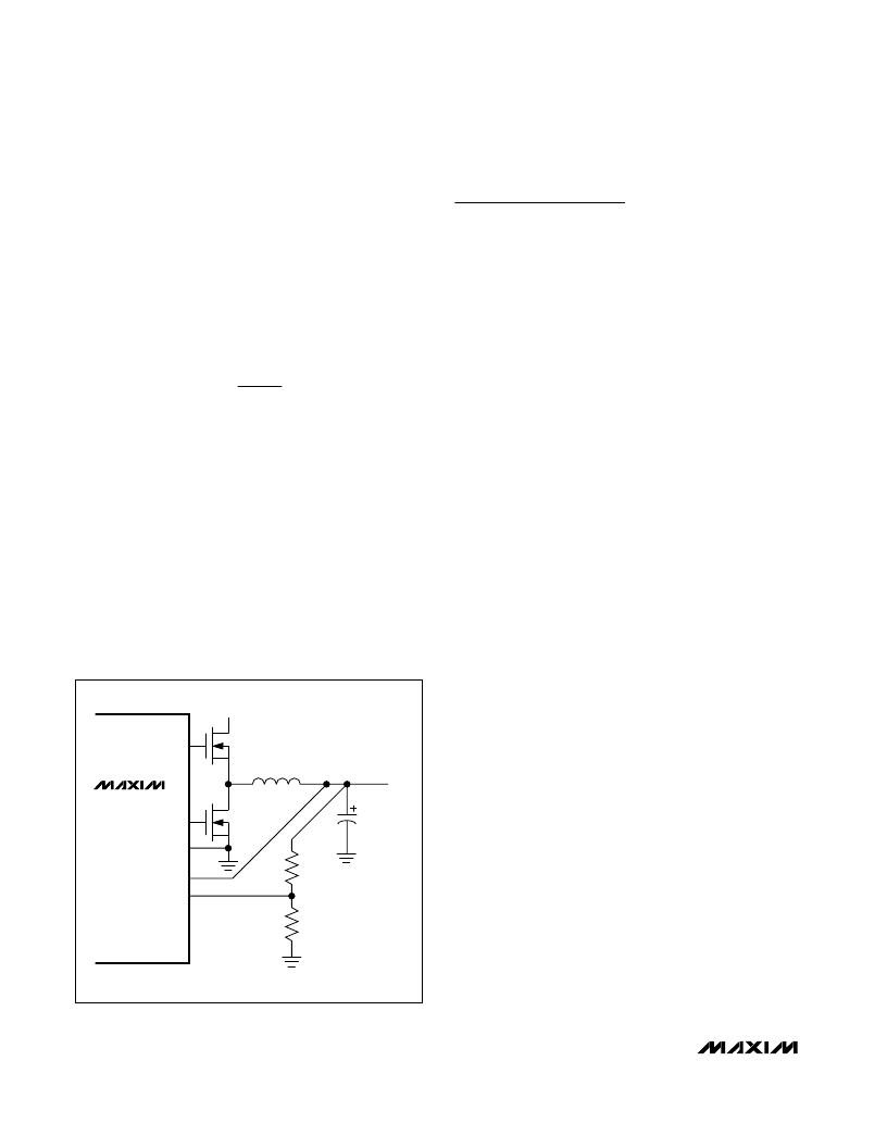
age-divider at FB_ between OUT_ and GND to adjust
the respective output voltage between 2V and 5.5V
(Figure 11). Choose R2 to be about 10k
and solve for
R1 using the equation:
where V
FB
= 2V nominal.
When using the adjustable output mode, set the 3.3V
SMPS lower than the 5V SMPS. LDO5 connects to OUT5
through an internal switch only when OUT5 is above the
LDO5 bootstrap-switch threshold (4.56V). LDO3 con-
nects to OUT3 through an internal switch only when
OUT3 is above the LDO3 bootstrap switch threshold
(2.91V). Bootstrapping is most effective when the fixed
output voltages are used. Once LDO_ is bootstrapped
from OUT_, the internal linear regulator turns off. This
reduces internal power dissipation and improves effi-
ciency when LDO_ is powered with a high input voltage.
Design Proc edure
Establish the input voltage range and maximum load
current before choosing an inductor and its associated
ripple-current ratio (LIR). The following four factors dic-
tate the rest of the design:
1)
Input Voltage Range.
The maximum value (V+
(MAX)
)
must accommodate the maximum AC adapter volt-
age. The minimum value (V+
(MIN)
) must account for
the lowest input voltage after drops due to connec-
tors, fuses, and battery selector switches. Lower input
voltages result in better efficiency.
2)
Maximum Load Current.
The peak load current
(I
LOAD(MAX)
) determines the instantaneous compo-
nent stress and filtering requirements, and thus dri-
ves output capacitor selection, inductor saturation
rating, and the design of the current-limit circuit.
The continuous load current (I
LOAD
) determines the
thermal stress and drives the selection of input
capacitors, MOSFETs, and other critical heat-con-
tributing components.
3)
Switching Frequency.
This choice determines the
basic trade-off between size and efficiency. The
optimal frequency is largely a function of maximum
input voltage and MOSFET switching losses. The
MAX1777 has a nominal switching frequency of
200kHz for the 5V SMPS and 300kHz for the 3.3V
SMPS. The MAX1977 has a nominal switching fre-
quency of 400kHz for the 5V SMPS and 500kHz for
the 3.3V SMPS. The MAX1999 has pin-selectable
switching frequency.
4)
Inductor Ripple Current Ratio (LIR).
LIR is the
ratio of the peak-peak ripple current to the average
inductor current. Size and efficiency trade-offs must
be considered when setting the inductor ripple cur-
rent ratio. Low inductor values cause large ripple
currents, resulting in the smallest size, but poor effi-
ciency and high output noise. The minimum practi-
cal inductor value is one that causes the circuit to
operate at critical conduction (where the inductor
current just touches zero with every cycle at maxi-
mum load). Inductor values lower than this grant no
further size reduction benefit.
The MAX1777/MAX1977/MAX1999s’ pulse-skipping
algorithm (
SKIP
= GND) initiates skip mode at the
critical conduction point. So the inductor’s operat-
ing point also determines the load current at which
PWM/PFM switchover occurs. The optimum point is
usually found between 20% and 50% ripple current.
R
R
V
V
OUT
FB
1
2
1
=
×
_
MAX1777
MAX1977
MAX1999
DH_
DL_
GND
OUT_
FB_
V+
R1
R2
V
OUT_
Figure 11. Setting V
OUT_
with a Resistor-Divider
相關(guān)PDF資料 |
PDF描述 |
|---|---|
| MAX1999EEI | High-Efficiency, Quad Output, Main Power- Supply Controllers for Notebook Computers |
| MAX1778 | 32-Bit Digital Signal Controller with ROM 100-LQFP -40 to 85 |
| MAX1880 | Quad-Output TFT LCD DC-DC Converters with Buffer |
| MAX1881 | Quad-Output TFT LCD DC-DC Converters with Buffer |
| MAX1882 | Quad-Output TFT LCD DC-DC Converters with Buffer |
相關(guān)代理商/技術(shù)參數(shù) |
參數(shù)描述 |
|---|---|
| MAX1977EEI+ | 功能描述:DC/DC 開關(guān)控制器 Quad Out Main Power Supply Controller RoHS:否 制造商:Texas Instruments 輸入電壓:6 V to 100 V 開關(guān)頻率: 輸出電壓:1.215 V to 80 V 輸出電流:3.5 A 輸出端數(shù)量:1 最大工作溫度:+ 125 C 安裝風(fēng)格: 封裝 / 箱體:CPAK |
| MAX1977EEI+T | 功能描述:DC/DC 開關(guān)控制器 Quad Out Main Power Supply Controller RoHS:否 制造商:Texas Instruments 輸入電壓:6 V to 100 V 開關(guān)頻率: 輸出電壓:1.215 V to 80 V 輸出電流:3.5 A 輸出端數(shù)量:1 最大工作溫度:+ 125 C 安裝風(fēng)格: 封裝 / 箱體:CPAK |
| MAX1977EEI-T | 功能描述:DC/DC 開關(guān)控制器 RoHS:否 制造商:Texas Instruments 輸入電壓:6 V to 100 V 開關(guān)頻率: 輸出電壓:1.215 V to 80 V 輸出電流:3.5 A 輸出端數(shù)量:1 最大工作溫度:+ 125 C 安裝風(fēng)格: 封裝 / 箱體:CPAK |
| MAX1977EEI-TG068 | 制造商:Rochester Electronics LLC 功能描述: 制造商:Maxim Integrated Products 功能描述: |
| MAX1978ETM | 功能描述:電壓模式 PWM 控制器 RoHS:否 制造商:Texas Instruments 輸出端數(shù)量:1 拓?fù)浣Y(jié)構(gòu):Buck 輸出電壓:34 V 輸出電流: 開關(guān)頻率: 工作電源電壓:4.5 V to 5.5 V 電源電流:600 uA 最大工作溫度:+ 125 C 最小工作溫度:- 40 C 封裝 / 箱體:WSON-8 封裝:Reel |
發(fā)布緊急采購(gòu),3分鐘左右您將得到回復(fù)。