- 您現(xiàn)在的位置:買賣IC網(wǎng) > PDF目錄9499 > MAX1407CAI+ (Maxim Integrated Products)IC DAS 16BIT LP 28-SSOP PDF資料下載
參數(shù)資料
| 型號: | MAX1407CAI+ |
| 廠商: | Maxim Integrated Products |
| 文件頁數(shù): | 15/48頁 |
| 文件大?。?/td> | 0K |
| 描述: | IC DAS 16BIT LP 28-SSOP |
| 產(chǎn)品培訓(xùn)模塊: | Lead (SnPb) Finish for COTS Obsolescence Mitigation Program |
| 標準包裝: | 46 |
| 類型: | 數(shù)據(jù)采集系統(tǒng)(DAS) |
| 分辨率(位): | 16 b |
| 采樣率(每秒): | 60 |
| 數(shù)據(jù)接口: | 串行 |
| 電壓電源: | 模擬和數(shù)字 |
| 電源電壓: | 2.7 V ~ 3.6 V |
| 工作溫度: | 0°C ~ 70°C |
| 安裝類型: | 表面貼裝 |
| 封裝/外殼: | 28-SSOP(0.209",5.30mm 寬) |
| 供應(yīng)商設(shè)備封裝: | 28-SSOP |
| 包裝: | 管件 |
第1頁第2頁第3頁第4頁第5頁第6頁第7頁第8頁第9頁第10頁第11頁第12頁第13頁第14頁當(dāng)前第15頁第16頁第17頁第18頁第19頁第20頁第21頁第22頁第23頁第24頁第25頁第26頁第27頁第28頁第29頁第30頁第31頁第32頁第33頁第34頁第35頁第36頁第37頁第38頁第39頁第40頁第41頁第42頁第43頁第44頁第45頁第46頁第47頁第48頁
MAX1407/MAX1408/MAX1409/MAX1414
Low-Power, 16-Bit Multichannel DAS with
Internal Reference,10-Bit DACs, and RTC
22
______________________________________________________________________________________
Signal Detect
The INT pin will also go low and stay low when the dif-
ferential voltage on the selected analog inputs exceeds
the signal-detect comparator trip threshold (0mV for the
MAX1407/MAX1408/MAX1409 and 50mV for the
MAX1414). This will latch the SDC bit of the Status reg-
ister to one. Additional signal detect interrupts cannot
be generated unless the SDC bit is cleared. To clear
the SDC bit, the Status register must be read and the
input must be below the signal-detect threshold.
Powering down the signal detect-comparator without
reading the Status register will also clear the SDC bit.
Similar to the power-up case, INT goes high when the
device detects a start bit through the serial interface
from the P.
Time of Day Alarm
If the device is in Sleep mode, the alarm will wake up
the device and set the ALIRQ bit. INT is asserted when
the PLL is turned on. If an alarm occurs while the
device is awake (BIASE = 1), the ALIRQ bit will be set
and INT will go low. INT remains low until the device
detects a start bit through the serial interface from the
P. ALIRQ is reset to 0 when any alarm register is read
or written to.
Shutdown (S
SH
HD
DN
N)
SHDN is an active-low output that can be used to con-
trol an external power supply. Powering up the PLL
(PLLE = 1) or writing a “1” to the SHDE bit of the
Power2 register causes SHDN to go high. SHDN goes
low when the SHDE bit is set to 0 only if the PLL is pow-
ered down (PLLE = 0). The SHDN output stays high for
2.93ms (tDPD) after receiving a power-down command,
allowing the external power supply to stay alive so that
the P can properly complete a shutdown sequence.
SHDN is not available on the MAX1409. Note: Entering
Sleep mode automatically sets PLLE and SHDE to 0.
Any wake-up event will cause SHDN to go high. (See
Wake-Up section.)
Data Ready (D
DR
RD
DY
Y)
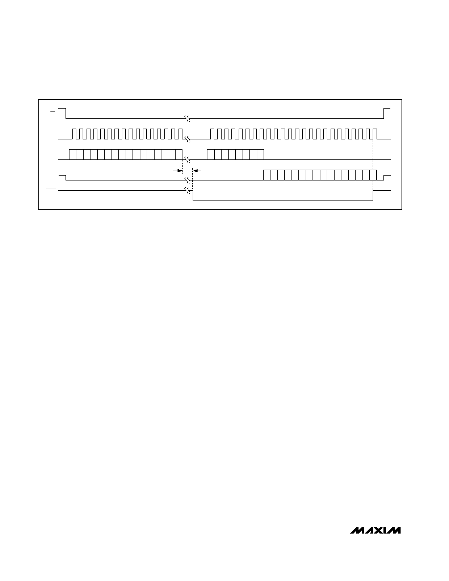
This pin will go low and stay low upon completion of an
ADC conversion or end of an ADC calibration. This sig-
nals the P that a valid conversion or calibration result
has been written to the DATA or the OFFSET register.
The DRDY pin goes high either when the P has fin-
ished reading the conversion/calibration result on the
last rising edge of SCLK (see Figure 8), or when the
next conversion result is about to be written to the
DATA register. When no read operation is performed,
DRDY pulses at 60Hz with a pulse high time of
162.76s (or 30Hz with a pulse high time of 325.52s)
DRDY is not available on the MAX1409. To see when
the ADC has completed a normal conversion or a cali-
bration conversion for the MAX1409, check the status
of the ADD bit in the Status register.
Serial Digital Interface
The SPI/QSPI/MICROWIRE-serial interface consists of
chip select (CS), serial clock (SCLK), data in (DIN), and
data out (DOUT) (See Figure 9). The serial interface
provides access to 29 on-chip registers, allowing con-
trol to all the power modes and functional blocks,
including the ADCs, DACs, and RTC. Table 2 lists the
address and read/write accessibility of all the registers.
A logic high on CS three-states DOUT and causes the
MAX1407/MAX1408/MAX1409/MAX1414 to ignore any
signals on SCLK and DIN. To clock data into or out of
the internal shift register, drive CS low. SCLK synchro-
nizes the data transfer. The rising edge of SCLK clocks
DIN into the shift register, and the falling edge of SCLK
Figure 8. ADC Conversion Timing Diagram
CS
SCLK
DIN
DOUT
1
0 A4 A3 A2 A1 A0 x
1
1 A4 A3 A2 A1 A0 x
D7 D6 D5 D4 D3 D2 D1 D0
D8
D9
D15 D14 D13 D12 D11 D10
DRDY
D7 D6 D5 D4 D3 D2 D1 D0
ADC
CONV
相關(guān)PDF資料 |
PDF描述 |
|---|---|
| MAX1414CAI+ | IC DAS 16BIT LP 28-SSOP |
| NBXDPA019LN1TAG | IC CLK XO LVDS 125/250MHZ 6CLCC |
| MAX181CCQH+D | IC DAS 12BIT 100KSPS 44-PLCC |
| 74AC138SC | IC DECODER/DEMUX 1OF8 16-SOIC |
| MAX181CCQH-D | IC DAS 6CH 12BIT 100KHZ 44-PLCC |
相關(guān)代理商/技術(shù)參數(shù) |
參數(shù)描述 |
|---|---|
| MAX1407CAI+ | 功能描述:ADC / DAC多通道 16-Bit 4Ch 60sps 1.35V Precision ADC RoHS:否 制造商:Texas Instruments 轉(zhuǎn)換速率: 分辨率:8 bit 接口類型:SPI 電壓參考: 電源電壓-最大:3.6 V 電源電壓-最小:2 V 最大工作溫度:+ 85 C 安裝風(fēng)格:SMD/SMT 封裝 / 箱體:VQFN-40 |
| MAX1407CAI+T | 功能描述:ADC / DAC多通道 16-Bit 4Ch 60sps 1.35V Precision ADC RoHS:否 制造商:Texas Instruments 轉(zhuǎn)換速率: 分辨率:8 bit 接口類型:SPI 電壓參考: 電源電壓-最大:3.6 V 電源電壓-最小:2 V 最大工作溫度:+ 85 C 安裝風(fēng)格:SMD/SMT 封裝 / 箱體:VQFN-40 |
| MAX1407CAI-T | 功能描述:ADC / DAC多通道 RoHS:否 制造商:Texas Instruments 轉(zhuǎn)換速率: 分辨率:8 bit 接口類型:SPI 電壓參考: 電源電壓-最大:3.6 V 電源電壓-最小:2 V 最大工作溫度:+ 85 C 安裝風(fēng)格:SMD/SMT 封裝 / 箱體:VQFN-40 |
| MAX1407EAI+ | 制造商:Maxim Integrated Products 功能描述:LOW-POWER 16-BIT MULTICHANNEL DAS - Rail/Tube |
| MAX1407EAI+T | 制造商:Maxim Integrated Products 功能描述:LOW-POWER 16-BIT MULTICHANNEL DAS - Tape and Reel |
發(fā)布緊急采購,3分鐘左右您將得到回復(fù)。