- 您現(xiàn)在的位置:買賣IC網(wǎng) > PDF目錄224146 > M470T5663EH3-CF7 DDR DRAM MODULE, ZMA200 PDF資料下載
參數(shù)資料
| 型號: | M470T5663EH3-CF7 |
| 元件分類: | DRAM |
| 英文描述: | DDR DRAM MODULE, ZMA200 |
| 封裝: | ROHS COMPLIANT, SODIMM-200 |
| 文件頁數(shù): | 4/22頁 |
| 文件大小: | 401K |
| 代理商: | M470T5663EH3-CF7 |
Rev. 1.0 August 2008
SODIMM
DDR2 SDRAM
12 of 22
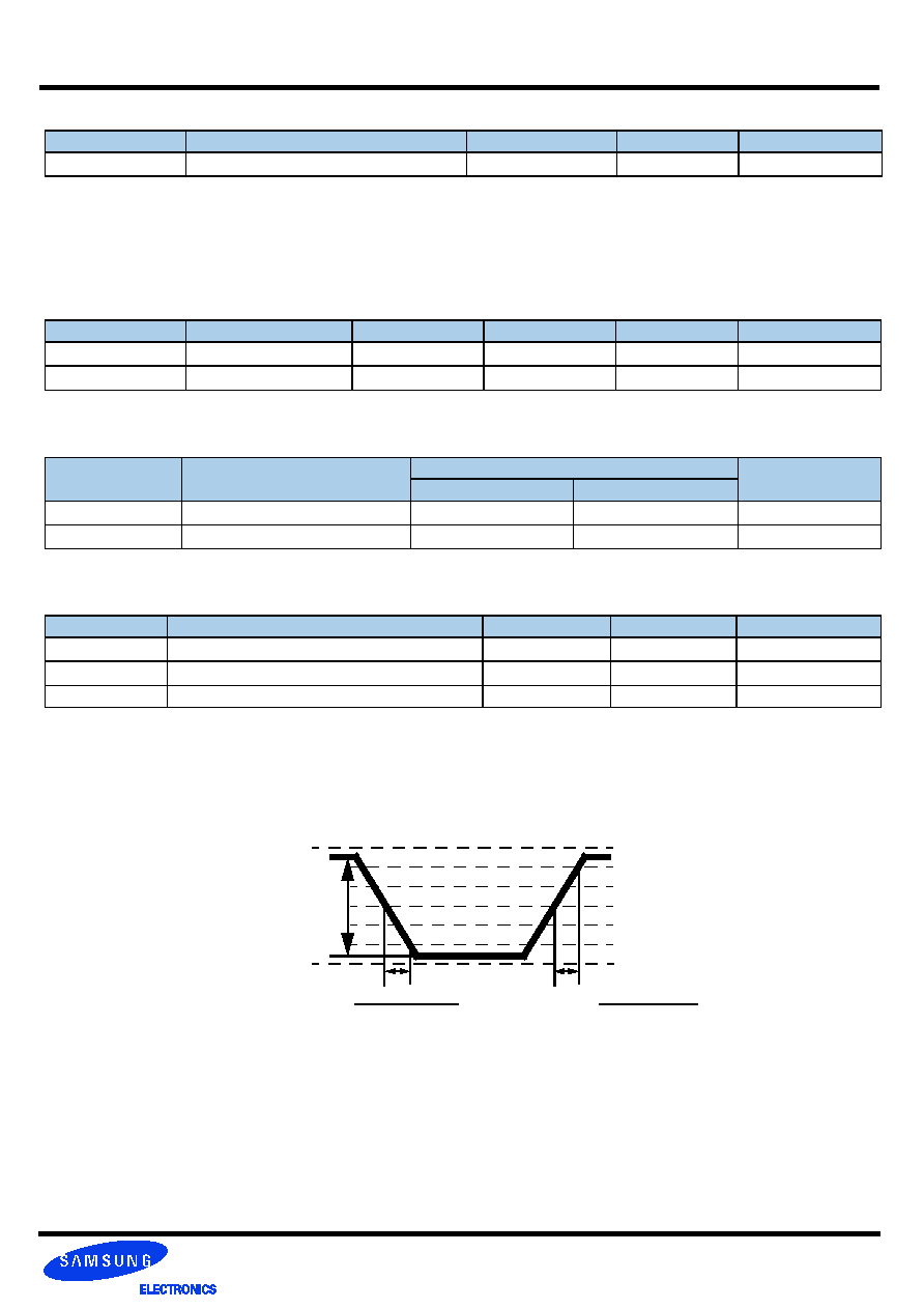
Note:
1. Input waveform timing is referenced to the input signal crossing through the VIH/IL(AC) level applied to the device under test.
2. The input signal minimum slew rate is to be maintained over the range from VREF to VIH(AC) min for rising edges and the range from VREF to VIL(AC)
max for falling edges as shown in the below figure.
3. AC timings are referenced with input waveforms switching from VIL(AC) to VIH(AC) on the positive transitions and VIH(AC) to VIL(AC) on the negative
transitions.
Symbol
Condition
Value
Units
Notes
VREF
Input reference voltage
0.5 * VDDQ
V1
VSWING(MAX)
Input signal maximum peak to peak swing
1.0
V
1
SLEW
Input signal minimum slew rate
1.0
V/ns
2, 3
VDDQ
VIH(AC) min
VIH(DC) min
VREF
VIL(DC) max
VIL(AC) max
VSS
< AC Input Test Signal Waveform >
VSWING(MAX)
delta TR
delta TF
VREF - VIL(AC) max
delta TF
Falling Slew =
Rising Slew =
VIH(AC) min - VREF
delta TR
Note :
1. Operating Temperature is the case surface temperature on the center/top side of the DRAM. For the measurement conditions, please refer to
JESD51.2 standard.
2. At 85 - 95
°C operation temperature range, doubling refresh commands in frequency to a 32ms period ( tREFI=3.9 us ) is required, and to enter to self
refresh mode at this temperature range, an EMRS command is required to change internal refresh rate.
Symbol
Parameter
Rating
Units
Notes
TOPER
Operating Temperature
0 to 95
°C
1, 2
9.3 Input DC Logic Level
Symbol
Parameter
Min.
Max.
Units
Notes
VIH(DC)
DC input logic high
VREF + 0.125
VDDQ + 0.3
V
VIL(DC)
DC input logic low
- 0.3
VREF - 0.125
V
9.4 Input AC Logic Level
Symbol
Parameter
DDR2-667, DDR2-800
Units
Min.
Max.
VIH(AC)
AC input logic high
VREF + 0.200
V
VIL(AC)
AC input logic low
VREF - 0.200
V
9.5 AC Input Test Conditions
9.2 Operating Temperature Condition
相關(guān)PDF資料 |
PDF描述 |
|---|---|
| M470T6464EHS-CE6 | DDR DRAM MODULE, ZMA200 |
| M470T6464EHS-LF7 | DDR DRAM MODULE, ZMA200 |
| M48T128V | 3.3V-5V 1 Mbit 128Kb x8 TIMEKEEPER SRAM |
| M48T12 | 16 Kbit 2Kb x8 TIMEKEEPER[ SRAM |
| M48T12-150PC1 | 16 Kbit 2Kb x8 TIMEKEEPER[ SRAM |
相關(guān)代理商/技術(shù)參數(shù) |
參數(shù)描述 |
|---|---|
| M470T5663FB3 | 制造商:SAMSUNG 制造商全稱:Samsung semiconductor 功能描述:DDR2 SDRAM Memory |
| M470T5663FB3-CE600 | 制造商:Samsung Semiconductor 功能描述:SDRAM DDR2, 2GB 333MHZ, 1.8V - Trays |
| M470T5663FB3-CF700 | 制造商:Samsung Semiconductor 功能描述: |
| M470T5663QZ3-CE600 | 制造商:Samsung SDI 功能描述:DRAM Module DDR2 SDRAM 2GByte 200SODIMM |
| M470T5663QZ3-CF700 | 制造商:Samsung SDI 功能描述:DRAM Module DDR2 SDRAM 2GByte 200SODIMM |
發(fā)布緊急采購,3分鐘左右您將得到回復(fù)。