- 您現(xiàn)在的位置:買賣IC網(wǎng) > PDF目錄370849 > M37754M8C-XXXHP (Mitsubishi Electric Corporation) SINGLE-CHIP 16BIT CMOS MICROCOMPUTER PDF資料下載
參數(shù)資料
| 型號: | M37754M8C-XXXHP |
| 廠商: | Mitsubishi Electric Corporation |
| 英文描述: | SINGLE-CHIP 16BIT CMOS MICROCOMPUTER |
| 中文描述: | 單芯片16位微機的CMOS |
| 文件頁數(shù): | 66/114頁 |
| 文件大小: | 1116K |
| 代理商: | M37754M8C-XXXHP |
第1頁第2頁第3頁第4頁第5頁第6頁第7頁第8頁第9頁第10頁第11頁第12頁第13頁第14頁第15頁第16頁第17頁第18頁第19頁第20頁第21頁第22頁第23頁第24頁第25頁第26頁第27頁第28頁第29頁第30頁第31頁第32頁第33頁第34頁第35頁第36頁第37頁第38頁第39頁第40頁第41頁第42頁第43頁第44頁第45頁第46頁第47頁第48頁第49頁第50頁第51頁第52頁第53頁第54頁第55頁第56頁第57頁第58頁第59頁第60頁第61頁第62頁第63頁第64頁第65頁當(dāng)前第66頁第67頁第68頁第69頁第70頁第71頁第72頁第73頁第74頁第75頁第76頁第77頁第78頁第79頁第80頁第81頁第82頁第83頁第84頁第85頁第86頁第87頁第88頁第89頁第90頁第91頁第92頁第93頁第94頁第95頁第96頁第97頁第98頁第99頁第100頁第101頁第102頁第103頁第104頁第105頁第106頁第107頁第108頁第109頁第110頁第111頁第112頁第113頁第114頁
66
PRELIMINARY
Notice: This is not a final specification.
Some parametric limits are subject to change.
MITSUBISHI MICROCOMPUTERS
M37754M8C-XXXGP, M37754M8C-XXXHP
M37754S4CGP, M37754S4CHP
SINGLE-CHIP 16-BIT CMOS MICROCOMPUTER
CLOCK GENERATING CIRCUIT
The clock generating circuit makes basic clocks, which activate the
central processing unit (CPU), bus interface unit (BIU) and internal
peripheral devices, of an oscillation circuit output. Figure 82 shows
the block diagram of the clock generating circuit.
The clock source
φ
1
to activate internal peripheral devices, the clock
source
φ
BIU
to activate the bus interface unit and the clock source
φ
CPU
to activate the CPU are made of an clock input to the X
IN
pin.
When bit 6 (clock source select bit) of processor mode register 1 is
“0”, the clock which is obtained by dividing an input clock to the X
IN
pin by 2 becomes the clock source
φ
1
. When bit 6 is “1”, the clock
which is an input clock to the X
IN
pin becomes the clock source
φ
1
as it is. When bit 2 (clock source for peripheral devices select bit) is
“0”, the clock source
φ
1
which is more divided by 2 becomes the
standard clock for peripheral devices. When bit 2 is “1”, the clock
source
φ
1
becomes the standard clock for peripheral devices as it
is.
The standard clock is more divided with the division circuit shown in
Figure 82 and the clocks having all kinds of frequencies are made.
Each internal peripheral device can select one of 4 clocks, Pf
2
, Pf
16
,
Pf
64
and Pf
512
, and use it.
Pf
2
means f(X
IN
), which is an oscillation circuit’s frequency, divided
by 2 when the clock source for peripheral devices select bit is “1”. It
means f(X
IN
) divided by 4 when that bit is “0”. In the case of
φ
1
> 12.5
MHz, fix the bit to “0”.
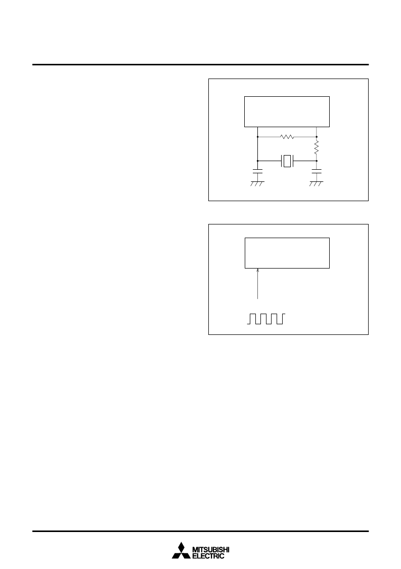
Figure 80 shows a circuit example using a ceramic (or quartz crys-
tal) resonator. Use the manufactures’ recommended values for con-
stants such as capacitance which differs for each resonator.
Figure 81 shows a circuit example inputting clocks externally. When
inputting clocks externally, setting bit 1 (clock external input select
bit) of particular function select register 0 (in Figure 83) to “1” makes
operation of the clock oscillation circuit stop, that is, the X
OUT
output
stays at “H”, and the current consumption reduce.
X
IN
R
f
X
OUT
R
d
C
IN
C
OUT
X
IN
External clock source
Vcc
Vss
X
OUT
Open
Fig. 80 Circuit example using a ceramic (or quartz crystal) resonator
Fig. 81 Circuit example inputting clocks externally
相關(guān)PDF資料 |
PDF描述 |
|---|---|
| M37754S4CGP | SINGLE-CHIP 16BIT CMOS MICROCOMPUTER |
| M37754S4CHP | SINGLE-CHIP 16BIT CMOS MICROCOMPUTER |
| M37754 | SINGLE-CHIP 16BIT CMOS MICROCOMPUTER |
| M37754M8C | Single Chip 16 Bits CMOS Microcomputer(16位單片機) |
| M37902F8CHP | DIODE SCHOTTKY DUAL COMMON-ANODE 25V 200mW 0.32V-vf 200mA-IFM 1mA-IF 2uA-IR SOT-23 3K/REEL |
相關(guān)代理商/技術(shù)參數(shù) |
參數(shù)描述 |
|---|---|
| M37754S4CGP | 制造商:MITSUBISHI 制造商全稱:Mitsubishi Electric Semiconductor 功能描述:SINGLE-CHIP 16BIT CMOS MICROCOMPUTER |
| M37754S4CHP | 制造商:RENESAS 制造商全稱:Renesas Technology Corp 功能描述:SINGLE-CHIP 16-BIT CMOS MICROCOMPUTER |
| M3775PR-H400CL | 制造商:Bonitron 功能描述:OVERVOLTAGE BRAKING RESISTOR |
| M3775RK-0.75A | 制造商:Bonitron 功能描述:OVERVOLTAGE BRAKING RESISTOR |
| M3775RK-C0.50A | 制造商:Bonitron 功能描述:OVERVOLTAGE BRAKING RESISTOR |
發(fā)布緊急采購,3分鐘左右您將得到回復(fù)。