- 您現(xiàn)在的位置:買賣IC網(wǎng) > PDF目錄370849 > M37754M8C-XXXGP (Mitsubishi Electric Corporation) SINGLE-CHIP 16BIT CMOS MICROCOMPUTER PDF資料下載
參數(shù)資料
| 型號: | M37754M8C-XXXGP |
| 廠商: | Mitsubishi Electric Corporation |
| 英文描述: | SINGLE-CHIP 16BIT CMOS MICROCOMPUTER |
| 中文描述: | 單芯片16位微機(jī)的CMOS |
| 文件頁數(shù): | 49/114頁 |
| 文件大小: | 1116K |
| 代理商: | M37754M8C-XXXGP |
第1頁第2頁第3頁第4頁第5頁第6頁第7頁第8頁第9頁第10頁第11頁第12頁第13頁第14頁第15頁第16頁第17頁第18頁第19頁第20頁第21頁第22頁第23頁第24頁第25頁第26頁第27頁第28頁第29頁第30頁第31頁第32頁第33頁第34頁第35頁第36頁第37頁第38頁第39頁第40頁第41頁第42頁第43頁第44頁第45頁第46頁第47頁第48頁當(dāng)前第49頁第50頁第51頁第52頁第53頁第54頁第55頁第56頁第57頁第58頁第59頁第60頁第61頁第62頁第63頁第64頁第65頁第66頁第67頁第68頁第69頁第70頁第71頁第72頁第73頁第74頁第75頁第76頁第77頁第78頁第79頁第80頁第81頁第82頁第83頁第84頁第85頁第86頁第87頁第88頁第89頁第90頁第91頁第92頁第93頁第94頁第95頁第96頁第97頁第98頁第99頁第100頁第101頁第102頁第103頁第104頁第105頁第106頁第107頁第108頁第109頁第110頁第111頁第112頁第113頁第114頁
49
PRELIMINARY
Notice: This is not a final specification.
Some parametric limits are subject to change.
MITSUBISHI MICROCOMPUTERS
M37754M8C-XXXGP, M37754M8C-XXXHP
M37754S4CGP, M37754S4CHP
SINGLE-CHIP 16-BIT CMOS MICROCOMPUTER
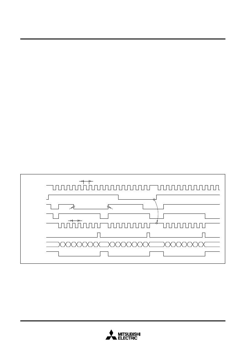
Transmission
Transmission is started when bit 0 (TEj flag) of UARTj Transmit/Re-
ceive control register 1 is “1”, bit 1 (TIj flag) of one is “0”, and CTSj
input is “L”. As shown in Figure 60, data is output from T
X
Dj pin each
time when transmission clock CLKj changes from “H” to “L”. The data
is output from the least significant bit.
The TIj flag indicates whether the transmit buffer register is empty or
not. It is cleared to “0” when data is written in the transmit buffer reg-
ister and set to “1” when the contents of the transmit buffer register is
transferred to the transmit register.
When the transmit register becomes empty after the contents has
been transmitted, data is transferred automatically from the transmit
buffer register to the transmit register if the next transmission start
condition is satisfied. If bit 2 of UARTj Transmit/Receive control reg-
ister 0 is “1”, CTSj input is ignored, and transmission start is con-
trolled only by the TEj flag and TIj flag. Once transmission has
started, the TEj flag, TIj flag, and CTSj signals are ignored until data
transmission completes. Therefore, transmission is not interrupt
when CTSj input is changed to “H” during transmission.
____
END
j signal (shown in Figure 60) is “H”.
Therefore, data can be transmitted continuously if the next transmis-
sion data is written in the transmit buffer register and TIj flag is
cleared to “0” before theT
END
j signal goes “H”.
Bit 3 (T
X
EPTYj flag) of UARTj Transmit/Receive control register 0
changes to “1” at the next cycle just after the T
END
j signal goes “H”
and changes to “0” when transmission starts. Therefore, this flag can
be used to determine whether data transmission has completed.
When the TIj flag changes from “0” to “1”, the interrupt request bit in
the UARTj transmit interrupt control register is set to “1”.
In only UART0, data can be output to a maximum of 3 external re-
ceive devices. This is realized under the condition in which the inter-
nal clock is selected and the transmission clock is output from one of
pins CLK
0
, CLKS
0
(multiplexed with R
X
D
0
) and CLKS
1
(multiplexed
with CTS
0
/RTS
0
). Make sure that do not switch the selection of the
clock during transmission. Figure 61 shows an external connection
example.
Plural output of transmit clock mode is set with bits 1 and 0 of the
particular function select register 1. Additionally, it is necessary to se-
lect the internal clock, disable CTS and RTS, receive and D-A output
with the UART0 Transmit/Receive mode register, UART0 Transmit/
Receive control registers 0 and 1, and A-D control register 1. Figure
62 shows the other registers bit configuration in plural output of trans-
mit clock mode and Figure 63 shows the particular function select
register 1 bit configuration .
Table 6 shows the function of the particular function select register
1’s bits 1 and 0, which is the output pin of transmit clock select bits:
TC
1
and TC
0
. According to this table, select the CLK
0
, CLKS
0
or
CLKS
1
pin corresponding to the contents of TC
1
and TC
0
, and out-
put the transmit clock.
Fig. 60 Clock synchronous serial I/O timing
Transmission
clock
TE
j
1/Pf
i
×
(n
+
1)
×
2
1/Pf
i
×
(n
+
1)
×
2
TI
j
CTS
j
Write in transmit buffer register
D
0
D
1
D
2
D
3
D
4
D
5
D
6
D
7
D
1
D
2
D
3
D
4
D
5
D
6
D
7
D
0
D
1
D
2
D
3
D
4
D
5
D
6
D
7
D
0
Transmit register
←
Transmit buffer register
Stopped because TE
j
= “0”
CLK
j
T
ENDj
T
X
D
j
T
X
EPTY
j
相關(guān)PDF資料 |
PDF描述 |
|---|---|
| M37754M8C-XXXHP | SINGLE-CHIP 16BIT CMOS MICROCOMPUTER |
| M37754S4CGP | SINGLE-CHIP 16BIT CMOS MICROCOMPUTER |
| M37754S4CHP | SINGLE-CHIP 16BIT CMOS MICROCOMPUTER |
| M37754 | SINGLE-CHIP 16BIT CMOS MICROCOMPUTER |
| M37754M8C | Single Chip 16 Bits CMOS Microcomputer(16位單片機(jī)) |
相關(guān)代理商/技術(shù)參數(shù) |
參數(shù)描述 |
|---|---|
| M37754M8C-XXXHP | 制造商:MITSUBISHI 制造商全稱:Mitsubishi Electric Semiconductor 功能描述:SINGLE-CHIP 16BIT CMOS MICROCOMPUTER |
| M37754S4CGP | 制造商:MITSUBISHI 制造商全稱:Mitsubishi Electric Semiconductor 功能描述:SINGLE-CHIP 16BIT CMOS MICROCOMPUTER |
| M37754S4CHP | 制造商:RENESAS 制造商全稱:Renesas Technology Corp 功能描述:SINGLE-CHIP 16-BIT CMOS MICROCOMPUTER |
| M3775PR-H400CL | 制造商:Bonitron 功能描述:OVERVOLTAGE BRAKING RESISTOR |
| M3775RK-0.75A | 制造商:Bonitron 功能描述:OVERVOLTAGE BRAKING RESISTOR |
發(fā)布緊急采購,3分鐘左右您將得到回復(fù)。