- 您現(xiàn)在的位置:買賣IC網(wǎng) > PDF目錄370849 > M37754M8C-XXXGP (Mitsubishi Electric Corporation) SINGLE-CHIP 16BIT CMOS MICROCOMPUTER PDF資料下載
參數(shù)資料
| 型號(hào): | M37754M8C-XXXGP |
| 廠商: | Mitsubishi Electric Corporation |
| 英文描述: | SINGLE-CHIP 16BIT CMOS MICROCOMPUTER |
| 中文描述: | 單芯片16位微機(jī)的CMOS |
| 文件頁數(shù): | 43/114頁 |
| 文件大小: | 1116K |
| 代理商: | M37754M8C-XXXGP |
第1頁第2頁第3頁第4頁第5頁第6頁第7頁第8頁第9頁第10頁第11頁第12頁第13頁第14頁第15頁第16頁第17頁第18頁第19頁第20頁第21頁第22頁第23頁第24頁第25頁第26頁第27頁第28頁第29頁第30頁第31頁第32頁第33頁第34頁第35頁第36頁第37頁第38頁第39頁第40頁第41頁第42頁當(dāng)前第43頁第44頁第45頁第46頁第47頁第48頁第49頁第50頁第51頁第52頁第53頁第54頁第55頁第56頁第57頁第58頁第59頁第60頁第61頁第62頁第63頁第64頁第65頁第66頁第67頁第68頁第69頁第70頁第71頁第72頁第73頁第74頁第75頁第76頁第77頁第78頁第79頁第80頁第81頁第82頁第83頁第84頁第85頁第86頁第87頁第88頁第89頁第90頁第91頁第92頁第93頁第94頁第95頁第96頁第97頁第98頁第99頁第100頁第101頁第102頁第103頁第104頁第105頁第106頁第107頁第108頁第109頁第110頁第111頁第112頁第113頁第114頁
43
PRELIMINARY
Notice: This is not a final specification.
Some parametric limits are subject to change.
MITSUBISHI MICROCOMPUTERS
M37754M8C-XXXGP, M37754M8C-XXXHP
M37754S4CGP, M37754S4CHP
SINGLE-CHIP 16-BIT CMOS MICROCOMPUTER
Pulse mode 0
This mode divides a pulse output port into 4 bits and 4 bits and indi-
vidually controls them.
When setting the pulse output mode select bit to “0”, and setting bits
2 and 1 to “0” and bit 0 to “1” of the waveform output select bits, four
of RTP1
3
, RTP1
2
, RTP1
1
, and RTP1
0
become the pulse output
ports with RTP1 selected.
When setting the pulse output mode select bit to “0”, and setting bits
2 and 0 to “0” and bit 1 to “1” of the waveform output select bits, four
of RTP0
3
, RTP0
2
, RTP0
1
, RTP0
0
become the pulse output ports
with RTP0 selected.
When setting the pulse output mode select bit to “0”, and setting bit
2 to “0” and bits 1 and 0 to “1” of the waveform output select bits,
the following two groups become the pulse output ports with RTP1
and RTP0 selected:
Four of RTP1
3
, RTP1
2
, RTP1
1
, RTP1
0
Four of RTP0
3
, RTP0
2
, RTP0
1
, RTP0
0
.
Each time the contents of timer A1 counter become 0000
16
, the
contents of pulse output data register 1 (low-order 4 bits at address
1C
16
) corresponding to RTP1
3
, RTP1
2
, RTP1
1
, RTP1
0
are output
from ports.
Each time the contents of timer A0 counter become 0000
16
, the
contents of pulse output data register 0 (low-order 4 bits at address
1D
16
) corresponding to RTP0
3
, RTP0
2
, RTP0
1
, RTP0
0
are output
from ports.
When writing “0” to the specified bit of pulse output data register, “L”
level is output from the pulse output port when the contents of cor-
responding timer counter become 0000
16
; when writing “1” to it, “H”
level is output from the pulse output port.
Note :
Only when bit 5 of the particular function select register 1
(in Fig. 15) is set to “1”, this register’s contents can be
changed from the status after reset (in Fig.76).
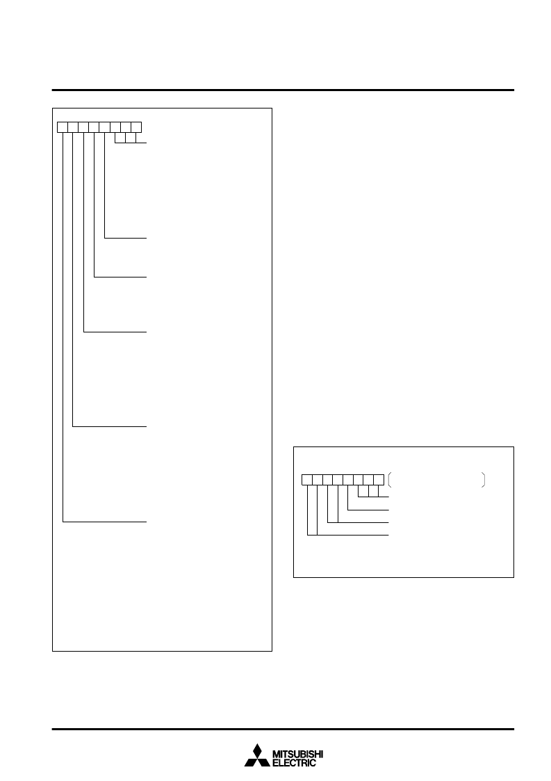
Waveform output mode register 1A
16
Waveform output select bits
000 : Parallel port
001 : RTP1 selected
(Valid in pulse mode 0)
010 : RTP0 selected
(Valid in pulse mode 0)
011 : In pulse mode 0
RTP1 and RTP0 selected
In pulse mode 1
RTP1, RTP0
3
, RTP0
2
,
RTP0
1
, RTP0
0
selected
Polarity select bit
(Valid for RTP0 in pulse mode 0)
0 : Positive polarity
1 : Negative polarity
Pulse width modulation select bit 0
(Valid for RTP1 in pulse mode 0;
Valid for RTP1, RTP0
3
, RTP0
2
in
pulse mode 1)
0 : No modulation by timer A2
1 : Modulation by timer A2
Pulse width modulation select bit 1*
(Valid in pulse mode 1)
0 : Modulation by timer A2
1 : Modulation for RTP0
3
, RTP0
2
by timer A2
Modulation for RTP1
1
, RTP1
0
by timer A3
Modulation for RTP1
3
, RTP1
2
by timer A4
* when selecting pulse mode 0, fix
this bit to “0”.
Waveform output control bit 0
0 : In pulse mode 0
Disable RTP0 waveform output
In pulse mode 1
Disable RTP0
output
1 : In pulse mode 0
Enable RTP0 waveform output
In pulse mode 1
Enable RTP0
1
, RTP0
0
waveform
output
1
, RTP0
0
waveform
Waveform output control bit 1
0 : In pulse mode 0
Disable RTP1 waveform output
In pulse mode 1
Disable RTP1, RTP0
3
, RTP0
2
waveform output
1 : In pulse mode 0
Enable RTP1 waveform output
In pulse mode 1
Enable RTP1, RTP0
waveform output
3
, RTP0
2
7
6
5
4
3
2
1
0
Address
Timer A0 mode register
Timer A1 mode register
56
16
57
16
100 : Fix to “100” in pulse output port mode
×
: Not used in pulse output port mode
00 : Fix to “00” in pulse output port mode
Clock source select bit
00 : Pf
2
selected
01 : Pf
16
selected
10 : Pf
64
selected
11 : Pf
512
selected
7
6
5
0
4
0
3
×
2
1
1
0
0
0
Address
Fig. 49 Bit configuration of waveform output mode register in pulse
output port mode
Fig. 50 Bit configuration of timer A1 and A0 mode registers in pulse
output port mode
相關(guān)PDF資料 |
PDF描述 |
|---|---|
| M37754M8C-XXXHP | SINGLE-CHIP 16BIT CMOS MICROCOMPUTER |
| M37754S4CGP | SINGLE-CHIP 16BIT CMOS MICROCOMPUTER |
| M37754S4CHP | SINGLE-CHIP 16BIT CMOS MICROCOMPUTER |
| M37754 | SINGLE-CHIP 16BIT CMOS MICROCOMPUTER |
| M37754M8C | Single Chip 16 Bits CMOS Microcomputer(16位單片機(jī)) |
相關(guān)代理商/技術(shù)參數(shù) |
參數(shù)描述 |
|---|---|
| M37754M8C-XXXHP | 制造商:MITSUBISHI 制造商全稱:Mitsubishi Electric Semiconductor 功能描述:SINGLE-CHIP 16BIT CMOS MICROCOMPUTER |
| M37754S4CGP | 制造商:MITSUBISHI 制造商全稱:Mitsubishi Electric Semiconductor 功能描述:SINGLE-CHIP 16BIT CMOS MICROCOMPUTER |
| M37754S4CHP | 制造商:RENESAS 制造商全稱:Renesas Technology Corp 功能描述:SINGLE-CHIP 16-BIT CMOS MICROCOMPUTER |
| M3775PR-H400CL | 制造商:Bonitron 功能描述:OVERVOLTAGE BRAKING RESISTOR |
| M3775RK-0.75A | 制造商:Bonitron 功能描述:OVERVOLTAGE BRAKING RESISTOR |
發(fā)布緊急采購,3分鐘左右您將得到回復(fù)。