- 您現(xiàn)在的位置:買賣IC網(wǎng) > PDF目錄45028 > M3455AG8FP 4-BIT, OTPROM, 6 MHz, MICROCONTROLLER, PQFP52 PDF資料下載
參數(shù)資料
| 型號: | M3455AG8FP |
| 元件分類: | 微控制器/微處理器 |
| 英文描述: | 4-BIT, OTPROM, 6 MHz, MICROCONTROLLER, PQFP52 |
| 封裝: | 10 X 10 MM, 0.65 MM PITCH, PLASTIC, LQFP-52 |
| 文件頁數(shù): | 124/150頁 |
| 文件大小: | 1818K |
| 代理商: | M3455AG8FP |
第1頁第2頁第3頁第4頁第5頁第6頁第7頁第8頁第9頁第10頁第11頁第12頁第13頁第14頁第15頁第16頁第17頁第18頁第19頁第20頁第21頁第22頁第23頁第24頁第25頁第26頁第27頁第28頁第29頁第30頁第31頁第32頁第33頁第34頁第35頁第36頁第37頁第38頁第39頁第40頁第41頁第42頁第43頁第44頁第45頁第46頁第47頁第48頁第49頁第50頁第51頁第52頁第53頁第54頁第55頁第56頁第57頁第58頁第59頁第60頁第61頁第62頁第63頁第64頁第65頁第66頁第67頁第68頁第69頁第70頁第71頁第72頁第73頁第74頁第75頁第76頁第77頁第78頁第79頁第80頁第81頁第82頁第83頁第84頁第85頁第86頁第87頁第88頁第89頁第90頁第91頁第92頁第93頁第94頁第95頁第96頁第97頁第98頁第99頁第100頁第101頁第102頁第103頁第104頁第105頁第106頁第107頁第108頁第109頁第110頁第111頁第112頁第113頁第114頁第115頁第116頁第117頁第118頁第119頁第120頁第121頁第122頁第123頁當前第124頁第125頁第126頁第127頁第128頁第129頁第130頁第131頁第132頁第133頁第134頁第135頁第136頁第137頁第138頁第139頁第140頁第141頁第142頁第143頁第144頁第145頁第146頁第147頁第148頁第149頁第150頁
Rev.1.02
Nov 26, 2008
Page 73 of 146
REJ03B0224-0102
455A Group
NOTES ON NOISE
Countermeasures against noise are described below.
The following countermeasures are effective against noise in
theory, however, it is necessary not only to take measures as
follows but to evaluate before actual use.
(1) Shortest wiring length
The wiring on a printed circuit board can function as an antenna
which feeds noise into the microcomputer.
The shorter the total wiring length (by mm unit), the less the
possibility of noise insertion into a microcomputer.
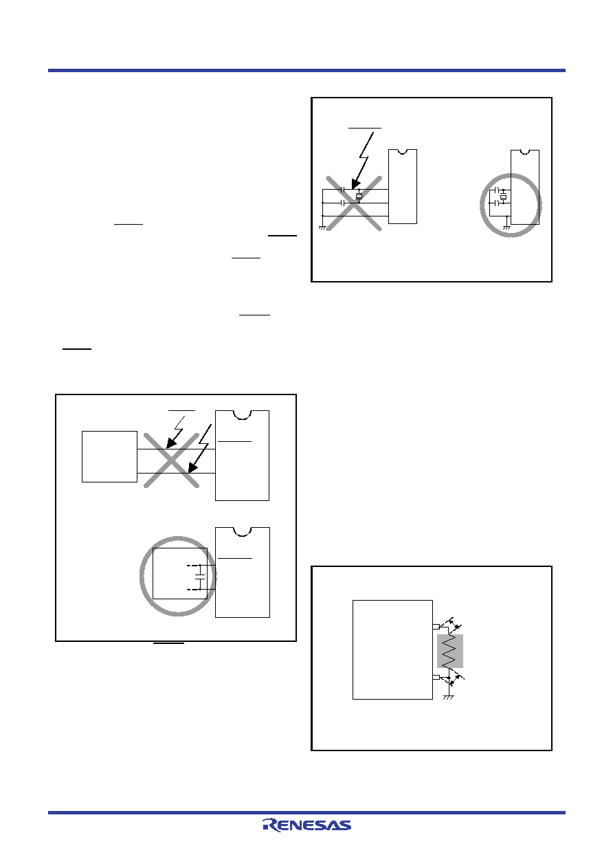
(1) Wiring for RESET input pin
Make the length of wiring which is connected to the RESET
input pin as short as possible.
Especially, connect a capacitor across the RESET input pin
and the VSS pin with the shortest possible wiring.
Reason
In order to reset a microcomputer correctly, 1 machine cycle or
more of the width of a pulse input into the RESET pin is
required.
If noise having a shorter pulse width than this is input to the
RESET input pin, the reset is released before the internal state
of the microcomputer is completely initialized.
This may cause a program runaway.
Fig 72. Wiring for the RESET input pin
(2) Wiring for clock input/output pins
Make the length of wiring which is connected to clock I/O
pins as short as possible.
Make the length of wiring across the grounding lead of a
capacitor which is connected to an oscillator and the VSS
pin of a microcomputer as short as possible.
Separate the VSS pattern only for oscillation from other
VSS patterns.
Fig 73. Wiring for clock I/O pins
Reason
If noise enters clock I/O pins, clock waveforms may be
deformed. This may cause a program failure or program
runaway.
Also, if a potential difference is caused by the noise between
the VSS level of a microcomputer and the VSS level of an
oscillator, the correct clock will not be inpu t in the
microcomputer.
(3) Wiring to CNVSS pin
Connect an approximately 5 k
resistor to the VPP pin and
also to the GND pattern supplied to the VSS pin with
shortest possible wiring.
Reason
The CNVSS pin is the power source input pin for the built-in
QzROM. When programming in the built-in QzROM, the
impedance of the CNVSS pin is low to allow the electric
current for writing flow into the QzROM. Because of this,
noise can enter easily. If noise enters the CNVSS pin, abnormal
instruction codes or data are read from the built-in QzROM,
which may cause a program runaway.
Fig 74. Wiring for CNVSS pin
RESET
Reset
circuit
Noise
VSS
N.G.
Reset
circuit
VSS
RESET
VSS
O.K.
Noise
XIN
XOUT
VSS
N.G.
XIN
XOUT
VSS
O.K.
CN V s s
V SS
T he shortest
about 5k
N ote: T his indicates pin.
(Note)
相關PDF資料 |
PDF描述 |
|---|---|
| M3455AGC-XXXFP | 4-BIT, OTPROM, 6 MHz, MICROCONTROLLER, PQFP52 |
| M3455AG8-XXXFP | 4-BIT, OTPROM, 6 MHz, MICROCONTROLLER, PQFP52 |
| M34570MD-XXXFP | 4-BIT, MROM, 2 MHz, MICROCONTROLLER, PDSO36 |
| M34570E8FP | 4-BIT, OTPROM, 2 MHz, MICROCONTROLLER, PDSO36 |
| M34583EDFP | 4-BIT, OTPROM, 6 MHz, MICROCONTROLLER, PQFP32 |
相關代理商/技術參數(shù) |
參數(shù)描述 |
|---|---|
| M3455AG8-XXXFP | 制造商:RENESAS 制造商全稱:Renesas Technology Corp 功能描述:SINGLE-CHIP 4-BIT CMOS MICROCOMPUTER |
| M3455AGCFP | 制造商:RENESAS 制造商全稱:Renesas Technology Corp 功能描述:SINGLE-CHIP 4-BIT CMOS MICROCOMPUTER |
| M3455AGC-XXXFP | 制造商:RENESAS 制造商全稱:Renesas Technology Corp 功能描述:SINGLE-CHIP 4-BIT CMOS MICROCOMPUTER |
| M3455-SL001 | 制造商:Alpha Wire 功能描述: |
| M3455-SL002 | 制造商:Alpha Wire 功能描述: |
發(fā)布緊急采購,3分鐘左右您將得到回復。