- 您現(xiàn)在的位置:買賣IC網(wǎng) > PDF目錄45027 > M34286G2-XXXGP 4-BIT, MROM, 4 MHz, MICROCONTROLLER, PDSO20 PDF資料下載
參數(shù)資料
| 型號: | M34286G2-XXXGP |
| 元件分類: | 微控制器/微處理器 |
| 英文描述: | 4-BIT, MROM, 4 MHz, MICROCONTROLLER, PDSO20 |
| 封裝: | 4.40 X 6.50 MM, 0.65 MM PITCH, PLASTIC, LSSOP-20 |
| 文件頁數(shù): | 28/30頁 |
| 文件大?。?/td> | 516K |
| 代理商: | M34286G2-XXXGP |
第1頁第2頁第3頁第4頁第5頁第6頁第7頁第8頁第9頁第10頁第11頁第12頁第13頁第14頁第15頁第16頁第17頁第18頁第19頁第20頁第21頁第22頁第23頁第24頁第25頁第26頁第27頁當(dāng)前第28頁第29頁第30頁
Rev.1.00
Aug 06, 2008
page 5 of 64
REJ03B0251-0100
4286 Group
CONNECTIONS OF UNUSED PINS
(Note when connecting to VSS and VDD)
Connect the unused pins to VSS or VDD at the shortest distance and use the thick wire against noise.
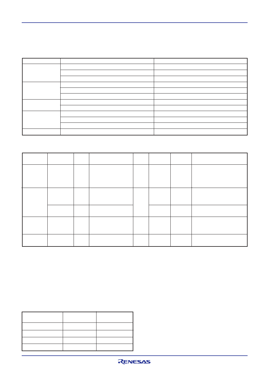
PORT FUNCTION
Control
bits
1 bit
Output:
2 bits
Input:
3 bits
4 bits
1 bit
Control
instructions
SD
RD
CLD
SZD
OEA
IAE
OGA
IAG
SCAR
RCAR
Control
registers
PU1, PU2
PU0
Output structure
P-channel open-drain
CMOS
Input/
Output
I/O
(8)
I/O
(2)
Input
(1)
I/O
(4)
Output
(1)
Remark
Pull-down function and
key-on wakeup function
(programmable)
Pull-down function and
key-on wakeup function
(programmable)
Pull-down function and
key-on wakeup function
(programmable)
Pin
D0–D7
E0
E1
E2
G0–G3
CARR
Port
Port D
Port E
Port G
Port CARR
DEFINITION OF CLOCK AND CYCLE
System clock (STCK)
The system clock is the source clock for controlling this product.
It can be selected as shown below whether to use the
Oscillation dividing instruction.
CCK, CCK2, or CCK4 instruction can be executed only once.
After one of their instruction is executed once, the operation is
same as the NOP instruction though the same or another
frequency dividing instruction is executed.
The system clock returns to its initial state (f(XIN)/8) when
system is returnd from RAM back-up mode.
Pin
D0–D7
E0, E1
E2
G0–G3
CARR
Connection
Open (Set the output latch to “1” ).
Open (Set the output latch to “0” ).
Connect to VDD.
Open (Set the output latch to “1” ).
Open (Set the output latch to “0” ).
Connect to VDD.
Open.
Connect to VSS.
Open (Set the output latch to “1” ).
Open (Set the output latch to “0” ).
Connect to VDD.
Open.
Usage condition
Pull-down transistor OFF.
System clock
f(XIN)/8
f(XIN)
f(XIN)/2
f(XIN)/4
Instruction clock
f(XIN)/32
f(XIN)/4
f(XIN)/8
f(XIN)/16
Oscillation dividing
instruction
No use
CCK used
CCK2 used
CCK4 used
Instruction clock (INSTCK)
The instruction clock is a signal derived by dividing the system
clock by 4, and is the basic clock for controlling CPU. The one
instruction clock cycle is equivalent to one machine cycle.
Machine cycle
The machine cycle is the cycle required to execute the
instruction.
相關(guān)PDF資料 |
PDF描述 |
|---|---|
| M34286G2GP | 4-BIT, MROM, 4 MHz, MICROCONTROLLER, PDSO20 |
| M34502M4-XXXFP | 4-BIT, MROM, 4.4 MHz, MICROCONTROLLER, PDSO24 |
| M34502M2-XXXFP | 4-BIT, MROM, 4.4 MHz, MICROCONTROLLER, PDSO24 |
| M34506M4-XXXFP | 4-BIT, MROM, MICROCONTROLLER, PDSO20 |
| M34506M2-XXXFP | 4-BIT, MROM, MICROCONTROLLER, PDSO20 |
相關(guān)代理商/技術(shù)參數(shù) |
參數(shù)描述 |
|---|---|
| M3429 SL001 | 制造商:Alpha Wire Company 功能描述:CBL 15PR 24AWG SLT 1000' |
| M3429 SL002 | 制造商:Alpha Wire Company 功能描述:CBL 15PR 24AWG SLT 500' |
| M3429 SL005 | 制造商:Alpha Wire Company 功能描述:CBL 15PR 24AWG SLT 100' |
| M34-2L | 制造商:BOWIN 制造商全稱:BOWIN 功能描述:SINGLE OUTPUT LED FLASHER IC |
| M342-SERIES | 制造商:未知廠家 制造商全稱:未知廠家 功能描述:Peripheral IC |
發(fā)布緊急采購,3分鐘左右您將得到回復(fù)。