- 您現(xiàn)在的位置:買賣IC網(wǎng) > PDF目錄45013 > M30280MAV-XXXHP 16-BIT, MROM, 20 MHz, MICROCONTROLLER, PQFP80 PDF資料下載
參數(shù)資料
| 型號(hào): | M30280MAV-XXXHP |
| 元件分類: | 微控制器/微處理器 |
| 英文描述: | 16-BIT, MROM, 20 MHz, MICROCONTROLLER, PQFP80 |
| 封裝: | 12 X 12 MM, 0.50 MM PITCH, PLASTIC, LQFP-80 |
| 文件頁數(shù): | 58/416頁 |
| 文件大小: | 3065K |
| 代理商: | M30280MAV-XXXHP |
第1頁第2頁第3頁第4頁第5頁第6頁第7頁第8頁第9頁第10頁第11頁第12頁第13頁第14頁第15頁第16頁第17頁第18頁第19頁第20頁第21頁第22頁第23頁第24頁第25頁第26頁第27頁第28頁第29頁第30頁第31頁第32頁第33頁第34頁第35頁第36頁第37頁第38頁第39頁第40頁第41頁第42頁第43頁第44頁第45頁第46頁第47頁第48頁第49頁第50頁第51頁第52頁第53頁第54頁第55頁第56頁第57頁當(dāng)前第58頁第59頁第60頁第61頁第62頁第63頁第64頁第65頁第66頁第67頁第68頁第69頁第70頁第71頁第72頁第73頁第74頁第75頁第76頁第77頁第78頁第79頁第80頁第81頁第82頁第83頁第84頁第85頁第86頁第87頁第88頁第89頁第90頁第91頁第92頁第93頁第94頁第95頁第96頁第97頁第98頁第99頁第100頁第101頁第102頁第103頁第104頁第105頁第106頁第107頁第108頁第109頁第110頁第111頁第112頁第113頁第114頁第115頁第116頁第117頁第118頁第119頁第120頁第121頁第122頁第123頁第124頁第125頁第126頁第127頁第128頁第129頁第130頁第131頁第132頁第133頁第134頁第135頁第136頁第137頁第138頁第139頁第140頁第141頁第142頁第143頁第144頁第145頁第146頁第147頁第148頁第149頁第150頁第151頁第152頁第153頁第154頁第155頁第156頁第157頁第158頁第159頁第160頁第161頁第162頁第163頁第164頁第165頁第166頁第167頁第168頁第169頁第170頁第171頁第172頁第173頁第174頁第175頁第176頁第177頁第178頁第179頁第180頁第181頁第182頁第183頁第184頁第185頁第186頁第187頁第188頁第189頁第190頁第191頁第192頁第193頁第194頁第195頁第196頁第197頁第198頁第199頁第200頁第201頁第202頁第203頁第204頁第205頁第206頁第207頁第208頁第209頁第210頁第211頁第212頁第213頁第214頁第215頁第216頁第217頁第218頁第219頁第220頁第221頁第222頁第223頁第224頁第225頁第226頁第227頁第228頁第229頁第230頁第231頁第232頁第233頁第234頁第235頁第236頁第237頁第238頁第239頁第240頁第241頁第242頁第243頁第244頁第245頁第246頁第247頁第248頁第249頁第250頁第251頁第252頁第253頁第254頁第255頁第256頁第257頁第258頁第259頁第260頁第261頁第262頁第263頁第264頁第265頁第266頁第267頁第268頁第269頁第270頁第271頁第272頁第273頁第274頁第275頁第276頁第277頁第278頁第279頁第280頁第281頁第282頁第283頁第284頁第285頁第286頁第287頁第288頁第289頁第290頁第291頁第292頁第293頁第294頁第295頁第296頁第297頁第298頁第299頁第300頁第301頁第302頁第303頁第304頁第305頁第306頁第307頁第308頁第309頁第310頁第311頁第312頁第313頁第314頁第315頁第316頁第317頁第318頁第319頁第320頁第321頁第322頁第323頁第324頁第325頁第326頁第327頁第328頁第329頁第330頁第331頁第332頁第333頁第334頁第335頁第336頁第337頁第338頁第339頁第340頁第341頁第342頁第343頁第344頁第345頁第346頁第347頁第348頁第349頁第350頁第351頁第352頁第353頁第354頁第355頁第356頁第357頁第358頁第359頁第360頁第361頁第362頁第363頁第364頁第365頁第366頁第367頁第368頁第369頁第370頁第371頁第372頁第373頁第374頁第375頁第376頁第377頁第378頁第379頁第380頁第381頁第382頁第383頁第384頁第385頁第386頁第387頁第388頁第389頁第390頁第391頁第392頁第393頁第394頁第395頁第396頁第397頁第398頁第399頁第400頁第401頁第402頁第403頁第404頁第405頁第406頁第407頁第408頁第409頁第410頁第411頁第412頁第413頁第414頁第415頁第416頁
13. Timer S
).
r
e
v
-
V
/.
r
e
v
-
T
(
p
u
o
r
G
8
2
/
C
6
1
M
page 130
0
9
3
f
o
7
0
2
,
0
3
.r
a
M
0
1
.
1
.
v
e
R
0
1
0
-
7
8
2
0
B
9
0
J
E
R
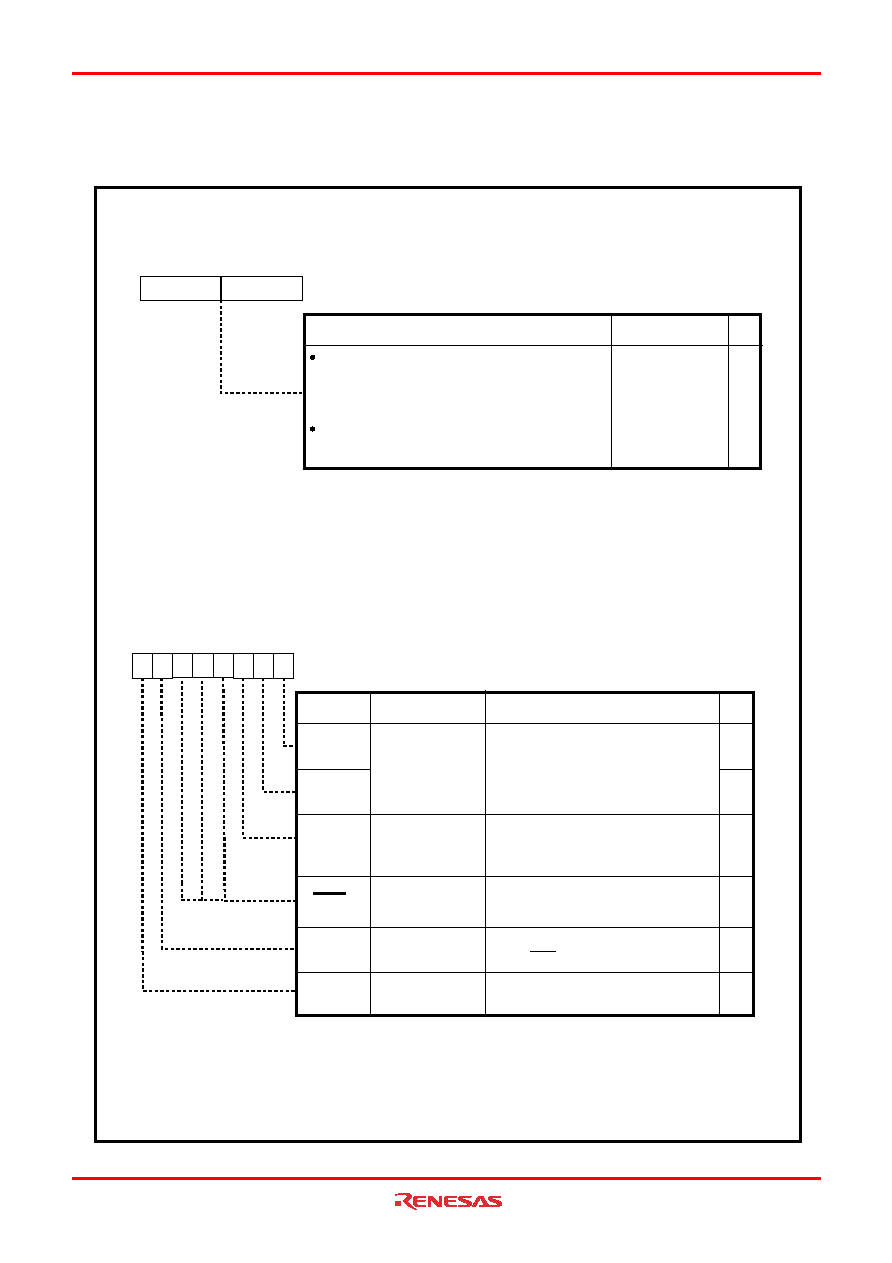
Figures 13.2
to 13.10 show registers associated with the IC/OC base timer, the time measurement func-
tion, and the waveform generating function.
Figure 13.2 G1BT and G1BCR0 Registers
Base Timer Register(1)
Symbol
Address
After Reset
G1BT
032116 - 032016
Indeterminate
RW
Function
(b7)
b0
Setting Range
000016 to FFFF16
b8
b15
b7
(b0)
When the base timer is operating:
When read, the value of base timer plus 1 can
be read. When write, the counter starts counting
from the value written. When the base timer is
reset, this register is set to "000016". (2)
When the base timer is reset:
This register is set to "000016" but a value read
is indeterminate. No value is written (2)
NOTES:
1. The G1BT register reflects the value of the base timer, synchronizing with the count source fBT1 cycles.
2. This base timer stops only when the BCK1 to BCK0 bits in the G1BCR0 register are set to "002" (count
source clock stop). The base timer operates when the BCK1 to BCK0 bits are set to other than "002".
When the BTS bit in the G1BCR1 register is set to "0", the base timer is reset continuously, and remaining
set to "000016". When the BTS bit is set to "1", this state is cleared and the timer starts counting.
Base Timer Control Register 0
Symbol
Address
After Reset
G1BCR0
032216
0016
RW
Bit Name
Function
Bit Symbol
: Clock stop
: Do not set to this value
: Two-phase input (1)
: f1 or f2 (2)
b1
0
1
b0
0
1
0
1
BCK0
BCK1
RST4
Count source
select bit
Channel 7 input
select bit
IT
Base timer
interrupt bit
0: Bit 15 overflow
1: Bit 14 overflow
CH7INSEL
0: Do not reset Base timer by matching
G1BTRR
1: Reset Base timer by matching
G1BTRR(3)
NOTES:
1. This setting can be used when bits UD1 to UD0 in the G1BCR1 register are set to 102 (two-
phase signal processing mode). Do not set bits BCK1 to BCK0 to 102 in other modes.
2. When the PCLK0 bit in the PCLKR register is set to 0, the count source is f2 cycles. And when
the PCLK0 bit is set to set to 1, the count source is f1 cycles.
3. When the RST4 bit is set to 1, set the RST1 bit in the G1BCR1 register to 0.
Base timer reset
cause select bit 4
0: P27/OUTC17/INPC17 pin
1: P17/INT5/INPC17/IDU pin
Reserved bit
Set to 0
(b5-b3)
RW
b7 b6 b5 b4 b3 b2 b1 b0
0
相關(guān)PDF資料 |
PDF描述 |
|---|---|
| M30281FATHP | 16-BIT, FLASH, 20 MHz, MICROCONTROLLER, PQFP64 |
| M30281M8V-XXXHP | 16-BIT, MROM, 20 MHz, MICROCONTROLLER, PQFP64 |
| M30281M8V-XXXHP | 16-BIT, MROM, 20 MHz, MICROCONTROLLER, PQFP64 |
| M30280FATHP | 16-BIT, FLASH, 20 MHz, MICROCONTROLLER, PQFP80 |
| M30281MAV-XXXHP | 16-BIT, MROM, 20 MHz, MICROCONTROLLER, PQFP64 |
相關(guān)代理商/技術(shù)參數(shù) |
參數(shù)描述 |
|---|---|
| M30280MA-XXXHP | 制造商:RENESAS 制造商全稱:Renesas Technology Corp 功能描述:16-BIT SINGLE-CHIP MICROCOMPUTER M16C FAMILY / M16C/Tiny SERIES |
| M30280MC-XXXHP | 制造商:RENESAS 制造商全稱:Renesas Technology Corp 功能描述:16-BIT SINGLE-CHIP MICROCOMPUTER M16C FAMILY / M16C/Tiny SERIES |
| M30281F6HP | 制造商:Renesas Electronics Corporation 功能描述:IC,microcontroller,M16C/Tiny,1 |
| M30281F6HP D3 | 制造商:Renesas Electronics Corporation 功能描述: |
| M30281F6HP D5 | 制造商:Renesas Electronics Corporation 功能描述: |
發(fā)布緊急采購,3分鐘左右您將得到回復(fù)。