- 您現(xiàn)在的位置:買賣IC網(wǎng) > PDF目錄384633 > LTUX (Linear Technology Corporation) 1-/2-Channel 20-Bit UPower No Latency ADCs in MSOP-10 PDF資料下載
參數(shù)資料
| 型號: | LTUX |
| 廠商: | Linear Technology Corporation |
| 英文描述: | 1-/2-Channel 20-Bit UPower No Latency ADCs in MSOP-10 |
| 中文描述: | 1-/2-Channel 20位ADC的無延遲UPower采用MSOP - 10 |
| 文件頁數(shù): | 25/32頁 |
| 文件大?。?/td> | 375K |
| 代理商: | LTUX |
第1頁第2頁第3頁第4頁第5頁第6頁第7頁第8頁第9頁第10頁第11頁第12頁第13頁第14頁第15頁第16頁第17頁第18頁第19頁第20頁第21頁第22頁第23頁第24頁當前第25頁第26頁第27頁第28頁第29頁第30頁第31頁第32頁
25
LTC2421/LTC2422
24212f
0.015ppm/
independent of capacitance at V
REF
, see
Figure 26.
In addition to the dynamic reference current, the V
REF
ESD
protection diodes have a temperature dependent leakage
current. This leakage current, nominally 1nA (
±
10nA max),
results in a fixed full-scale shift of 10
μ
V for a 10k source
resistance.
APPLICATIOU
W
U
U
The modulator contained within the LTC2421/LTC2422
can handle large-signal level perturbations without satu-
rating. Signal levels up to 40% of V
REF
do not saturate the
analog modulator. These signals are limited by the input
ESD protection to 300mV below ground and 300mV above
V
CC
.
Simple Basic Program for Interfacing to the
LTC2421/LTC2422
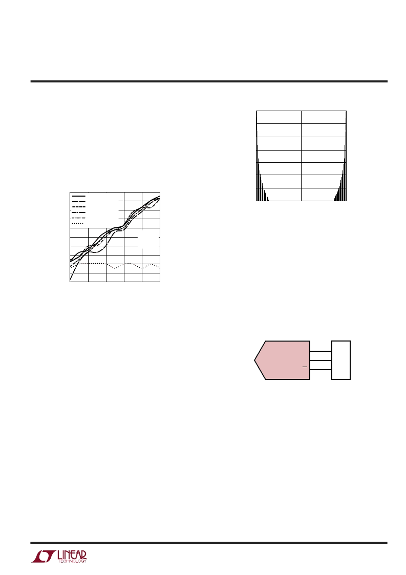
Figure 26. INL Error vs R
VREF
(Large C)
RESISTANCE AT V
REF
(
)
0
6
8
10
600
800
24212 F26
4
2
–2
–4
–6
–8
–10
200
400
1000
0
I
C
VREF
= 22
μ
F
C
VREF
= 10
μ
F
C
VREF
= 1
μ
F
C
VREF
= 0.1
μ
F
C
VREF
= 0.01
μ
F
C
VREF
= 0.001
μ
F
V
CC
= 5V
V
REF
= 5V
T
A
= 25
°
C
ANTIALIASING
One of the advantages delta-sigma ADCs offer over con-
ventional ADCs is on-chip digital filtering. Combined with
a large oversampling ratio, the LTC2421/LTC2422 signifi-
cantly simplify antialiasing filter requirements.
The digital filter provides very high rejection except at
integer multiples of the modulator sampling frequency
(f
S
), see Figure 27. The modulator sampling frequency is
256 F
O
, where F
O
is the notch frequency (typically 50Hz
or 60Hz). The bandwidth of signals not rejected by the
digital filter is narrow (
≈
0.2%) compared to the band-
width of the frequencies rejected.
As a result of the oversampling ratio (256) and the digital
filter, minimal (if any) antialias filtering is required in front
of the LTC2421/LTC2422. If passive RC components are
placed in front of the LTC2421/LTC2422, the input dy-
namic current should be considered (see Input Current
section). In cases where large effective RC time constants
are used, an external buffer amplifier may be required to
minimize the effects of input dynamic current.
Figure 27. Sinc
4
Filter Rejection
INPUT FREQUENCY
0
–60
–40
0
24212 F27
–80
–100
f
S
/2
f
S
–120
–140
–20
R
SCK
DTR
PC
SERIAL
PORT
CTS
RTS
SDO
LTC2421
LTC2422
CS
24212 F28
V
REF
V
IN
GND
Figure 28
”TINY.BAS V1.0 Copyright (C) 2000 by J. A. Dutra and LTC, All rights reseved'
NOTE this program generates 32 SCK’s for compatibility to 24-bit parts
'For use with most LTC24xy demo boards
designed for the PC Com Port, QBASIC
'Outputs are chan%,signneg%,d2400 (magnitude), PPM, and v (volts)
CLS : ON ERROR GOTO 4970
cport = 1: REM INPUT "com port number "; cport
GOSUB 1900: timestart$ = TIME$
mcr% = port + 4: msr% = port + 6
COLOR 15: LOCATE 3, 1: PRINT "Hit any key to stop… ";
FOR np = 1 TO 2000: OUT port, c0%: NEXT np: 'Power Via TxD
DO: '-------------------------START LOOP here--------
相關PDF資料 |
PDF描述 |
|---|---|
| LTUY | 1-/2-Channel 20-Bit UPower No Latency ADCs in MSOP-10 |
| LTUZ | 1-/2-Channel 20-Bit UPower No Latency ADCs in MSOP-10 |
| LTVA | 1-/2-Channel 20-Bit UPower No Latency ADCs in MSOP-10 |
| LTC2450 | Easy-to-Use, Ultra-Tiny 16-Bit ADC |
| LTC2450-1 | Easy-to-Use, Ultra-Tiny 16-Bit ADC |
相關代理商/技術參數(shù) |
參數(shù)描述 |
|---|---|
| LTUY | 制造商:LINER 制造商全稱:Linear Technology 功能描述:1-/2-Channel 20-Bit UPower No Latency ADCs in MSOP-10 |
| LTUZ | 制造商:LINER 制造商全稱:Linear Technology 功能描述:1-/2-Channel 20-Bit UPower No Latency ADCs in MSOP-10 |
| LTV-0501 | 功能描述:高速光耦合器 1Mbd High Speed Optocoupler RoHS:否 制造商:Avago Technologies 電流傳遞比: 最大波特率: 最大正向二極管電壓:1.75 V 最大反向二極管電壓:5 V 最大功率耗散:40 mW 最大工作溫度:+125 C 最小工作溫度:- 40 C 封裝 / 箱體:SOIC-5 封裝:Tube |
| LTV-0601 | 功能描述:高速光耦合器 10Mbd High Speed Optocoupler RoHS:否 制造商:Avago Technologies 電流傳遞比: 最大波特率: 最大正向二極管電壓:1.75 V 最大反向二極管電壓:5 V 最大功率耗散:40 mW 最大工作溫度:+125 C 最小工作溫度:- 40 C 封裝 / 箱體:SOIC-5 封裝:Tube |
| LTV-0701 | 功能描述:高速光耦合器 100 KBd High Speed Optocoupler RoHS:否 制造商:Avago Technologies 電流傳遞比: 最大波特率: 最大正向二極管電壓:1.75 V 最大反向二極管電壓:5 V 最大功率耗散:40 mW 最大工作溫度:+125 C 最小工作溫度:- 40 C 封裝 / 箱體:SOIC-5 封裝:Tube |
發(fā)布緊急采購,3分鐘左右您將得到回復。