- 您現(xiàn)在的位置:買賣IC網(wǎng) > PDF目錄384633 > LTUX (Linear Technology Corporation) 1-/2-Channel 20-Bit UPower No Latency ADCs in MSOP-10 PDF資料下載
參數(shù)資料
| 型號: | LTUX |
| 廠商: | Linear Technology Corporation |
| 英文描述: | 1-/2-Channel 20-Bit UPower No Latency ADCs in MSOP-10 |
| 中文描述: | 1-/2-Channel 20位ADC的無延遲UPower采用MSOP - 10 |
| 文件頁數(shù): | 22/32頁 |
| 文件大?。?/td> | 375K |
| 代理商: | LTUX |
第1頁第2頁第3頁第4頁第5頁第6頁第7頁第8頁第9頁第10頁第11頁第12頁第13頁第14頁第15頁第16頁第17頁第18頁第19頁第20頁第21頁當(dāng)前第22頁第23頁第24頁第25頁第26頁第27頁第28頁第29頁第30頁第31頁第32頁
22
LTC2421/LTC2422
24212f
resis
tance ground plane through a minimum length trace.
The use of multiple via holes is recommended to further
reduce the connection resistance.
In an alternative configuration, the GND pin of the con-
verter can be the single-point-ground in a single point
grounding system. The input signal ground, the reference
signal ground, the digital drivers ground (usually the digi-
tal ground) and the power supply ground (the analog
ground) should be connected in a star configuration with
the common point located as close to the GND pin as
possible.
The power supply current during the conversion state
should be kept to a minimum. This is achieved by restrict-
ing the number of digital signal transitions occurring dur-
ing this period.
While a digital input signal is in the range 0.5V to
(V
CC
–0.5V), the CMOS input receiver draws additional
current from the power supply. It should be noted that,
when any one of the digital input signals (F
O
, CS and SCK
in External SCK mode of operation) is within this range, the
LTC2421/LTC2422 power supply current may increase
even if the signal in question is at a valid logic level. For
micropower operation and in order to minimize the poten-
tial errors due to additional ground pin current, it is recom-
mended to drive all digital input signals to full CMOS levels
[V
IL
< 0.4V and V
OH
> (V
CC
– 0.4V)].
Severe ground pin current disturbances can also occur
due to the undershoot of fast digital input signals. Under-
shoot and overshoot can occur because of the imped-
ance mismatch at the converter pin when the transition
time of an external control signal is less than twice the
propagation delay from the driver to LTC2421/LTC2422.
For reference, on a regular FR-4 board, signal propaga-
tion velocity is approximately 183ps/inch for internal
traces and 170ps/inch for surface traces. Thus, a driver
generating a control signal with a minimum transition
time of 1ns must be connected to the converter pin through
a trace shorter than 2.5 inches. This problem becomes
particularly difficult when shared control lines are used
and multiple reflections may occur. The solution is to
carefully terminate all transmission lines close to their
characteristic impedance.
APPLICATIOU
W
U
U
Parallel termination near the LTC2421/LTC2422 pin will
eliminate this problem but will increase the driver power
dissipation. A series resistor between 27
and 56
placed
near the driver or near the LTC2421/LTC2422 pin will also
eliminate this problem without additional power dissipa-
tion. The actual resistor value depends upon the trace
impedance and connection topology.
Driving the Input and Reference
The analog input and reference of the typical delta-sigma
analog-to-digital converter are applied to a switched ca-
pacitor network. This network consists of capacitors switch-
ing between the analog input (V
IN
), ZS
SET
(Pin 5) and FS
SET
(Pin 2). The result is small current spikes seen at both V
IN
and V
REF
. A simplified input equivalent circuit is shown in
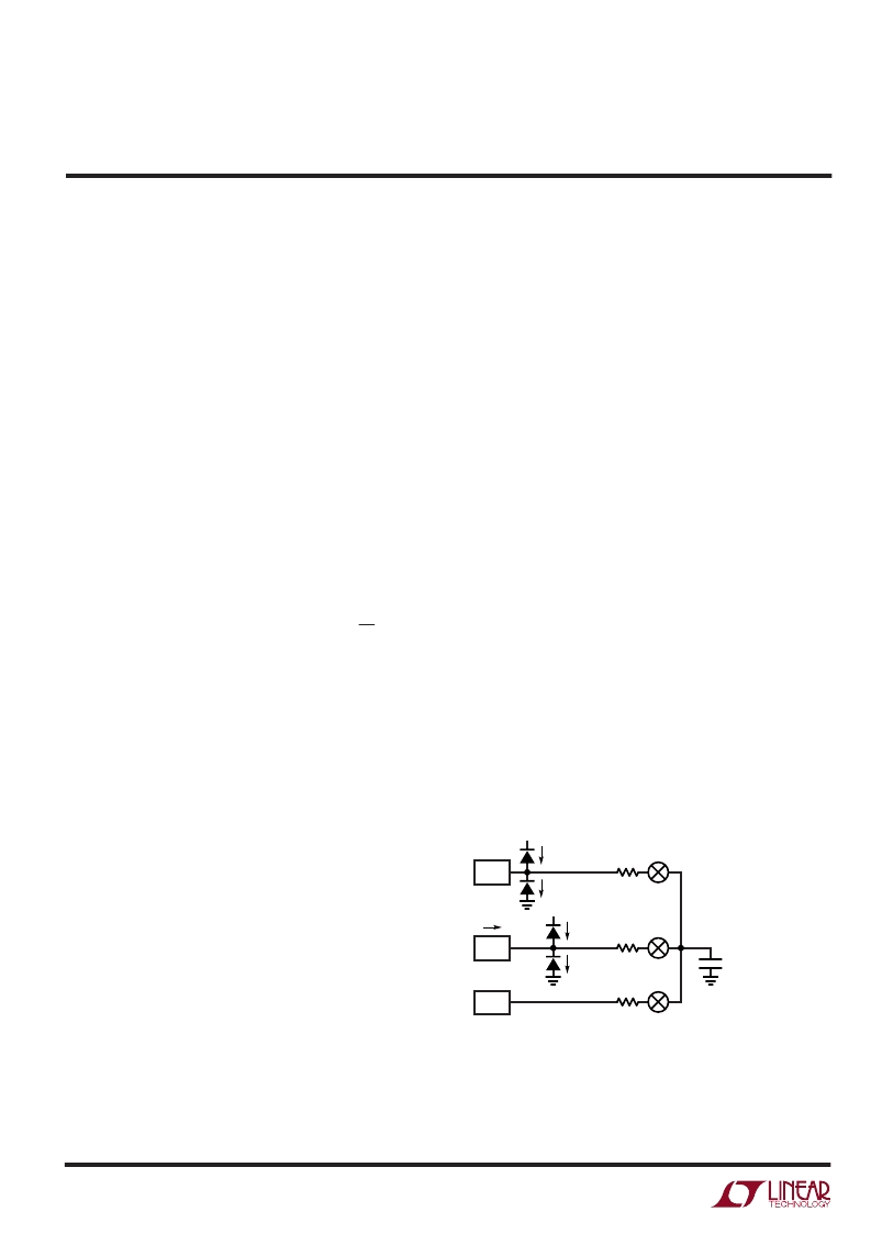
Figure 16.
The key to understanding the effects of this dynamic input
current is based on a simple first order RC time constant
model. Using the internal oscillator, the LTC2421/
LTC2422’s internal switched capacitor network is clocked
at 153,600Hz corresponding to a 6.5
μ
s sampling period.
Fourteen time constants are required each time a capacitor
is switched in order to achieve 1ppm settling accuracy.
Therefore, the equivalent time constant at V
IN
and V
REF
should be less than 6.5
μ
s/14 = 460ns in order to achieve
1ppm accuracy.
Figure 16. LTC2421/LTC2422 Equivalent Analog Input Circuit
V
REF
V
IN
V
CC
R
SW
5k
AVERAGE INPUT CURRENT:
I
IN
= 0.25(V
IN
– 0.5 V
REF
)fC
EQ
I
REF(LEAK)
I
REF(LEAK)
V
CC
R
SW
5k
C
1pF (TYP)
R
SW
5k
I
IN(LEAK)
I
IN
24212 F16
I
IN(LEAK)
SWITCHING FREQUENCY
f = 153.6kHz FOR INTERNAL OSCILLATOR (f
O
= LOGIC LOW OR HIGH)
f = f
EOSC
FOR EXTERNAL OSCILLATORS
GND
相關(guān)PDF資料 |
PDF描述 |
|---|---|
| LTUY | 1-/2-Channel 20-Bit UPower No Latency ADCs in MSOP-10 |
| LTUZ | 1-/2-Channel 20-Bit UPower No Latency ADCs in MSOP-10 |
| LTVA | 1-/2-Channel 20-Bit UPower No Latency ADCs in MSOP-10 |
| LTC2450 | Easy-to-Use, Ultra-Tiny 16-Bit ADC |
| LTC2450-1 | Easy-to-Use, Ultra-Tiny 16-Bit ADC |
相關(guān)代理商/技術(shù)參數(shù) |
參數(shù)描述 |
|---|---|
| LTUY | 制造商:LINER 制造商全稱:Linear Technology 功能描述:1-/2-Channel 20-Bit UPower No Latency ADCs in MSOP-10 |
| LTUZ | 制造商:LINER 制造商全稱:Linear Technology 功能描述:1-/2-Channel 20-Bit UPower No Latency ADCs in MSOP-10 |
| LTV-0501 | 功能描述:高速光耦合器 1Mbd High Speed Optocoupler RoHS:否 制造商:Avago Technologies 電流傳遞比: 最大波特率: 最大正向二極管電壓:1.75 V 最大反向二極管電壓:5 V 最大功率耗散:40 mW 最大工作溫度:+125 C 最小工作溫度:- 40 C 封裝 / 箱體:SOIC-5 封裝:Tube |
| LTV-0601 | 功能描述:高速光耦合器 10Mbd High Speed Optocoupler RoHS:否 制造商:Avago Technologies 電流傳遞比: 最大波特率: 最大正向二極管電壓:1.75 V 最大反向二極管電壓:5 V 最大功率耗散:40 mW 最大工作溫度:+125 C 最小工作溫度:- 40 C 封裝 / 箱體:SOIC-5 封裝:Tube |
| LTV-0701 | 功能描述:高速光耦合器 100 KBd High Speed Optocoupler RoHS:否 制造商:Avago Technologies 電流傳遞比: 最大波特率: 最大正向二極管電壓:1.75 V 最大反向二極管電壓:5 V 最大功率耗散:40 mW 最大工作溫度:+125 C 最小工作溫度:- 40 C 封裝 / 箱體:SOIC-5 封裝:Tube |
發(fā)布緊急采購,3分鐘左右您將得到回復(fù)。