- 您現(xiàn)在的位置:買賣IC網(wǎng) > PDF目錄44985 > LT3582EUD#PBF (LINEAR TECHNOLOGY CORP) 0.72 A SWITCHING REGULATOR, PQCC16 PDF資料下載
參數(shù)資料
| 型號: | LT3582EUD#PBF |
| 廠商: | LINEAR TECHNOLOGY CORP |
| 元件分類: | 穩(wěn)壓器 |
| 英文描述: | 0.72 A SWITCHING REGULATOR, PQCC16 |
| 封裝: | 3 X 3 MM, LEAD FREE, PLASTIC, MO-220WEED-2, QFN-16 |
| 文件頁數(shù): | 13/28頁 |
| 文件大小: | 315K |
| 代理商: | LT3582EUD#PBF |
第1頁第2頁第3頁第4頁第5頁第6頁第7頁第8頁第9頁第10頁第11頁第12頁當(dāng)前第13頁第14頁第15頁第16頁第17頁第18頁第19頁第20頁第21頁第22頁第23頁第24頁第25頁第26頁第27頁第28頁
LT3582/LT3582-5/LT3582-12
20
3582512fb
Output Disconnect Operating Limits
The LT3582 series has a PMOS output disconnect switch
connected between CAPP and VOUTP. During normal
operation, the switch is closed and current is internally
limited to about 155mA (see Figure 9). Make sure that the
output load current doesn’t exceed the PMOS current limit.
Exceeding the current limit causes a signicant rise in PMOS
power consumption which may damage the device.
During shutdown, the PMOS switch is open and CAPP is
isolated from VOUTP up to a voltage difference of 5-5.5V.
In most cases this allows VOUTP to discharge to ground.
However, when the Boost inductor input exceeds 5.5V, the
CAPP-VOUTPvoltagemayexceed5Vallowingsomecurrent
ow through the PMOS switch. In addition, applying CAPP-
VOUTP voltages in excess of 5.7V(typical) may activate
internal protection circuitry which turns the PMOS “on”
(see Figure 10). If the current is not limited, this can lead
to a sharp increase in the PMOS power consumption and
may damage the device. If this situation cannot be avoided,
limit PMOS power consumption to less than 1/3 Watt (about
50mA at 7V) to avoid damaging the device. Refer to the
Absolute Maximum Ratings table for maximum limits on
CAPP-VOUTP voltages and currents.
Improving Boost Converter Efciency
The efciency of the Boost converter can be improved by
shorting the CAPP pin to the VOUTP pin (see Figure 11). The
power loss in the PMOS disconnect circuit is then made
negligible. In most applications, the associated CAPP pin
capacitor can be removed and the larger VOUTP capacitor
can adequately lter the output voltage.
APPLICATIONS INFORMATION
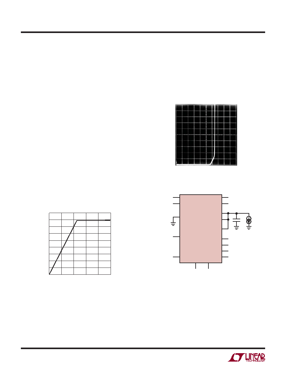
LT3582
VIN
CAPP
VOUTP
SDA
VPP
CA
SHDN
GND
SWN
VOUTN
3582512 F12
SCL
SWP
81
16
15
14
9
10
11
5
12
76
2
13
3
4
RAMPN
RAMPP
C1
ILOAD
Figure 10. PMOS Current vs Voltage During Shutdown
Figure 11. Improved Efciency
ICAPP-VOUTP
20μA/DIV
VCAPP-VOUTP 1V/DIV
3582512 F11
Figure 9. PMOS Current vs Voltage During Normal Operation
CAPP-VOUTP (mV)
0
100
200
400
300
500
0
20
40
100
80
120
140
60
160
180
PMOS
CURRENT
(mA)
3582512 F10
相關(guān)PDF資料 |
PDF描述 |
|---|---|
| LT3640EFE#TRPBF | 3.4 A DUAL SWITCHING CONTROLLER, 2350 kHz SWITCHING FREQ-MAX, PDSO28 |
| LT3640IFE#TRPBF | 3.4 A DUAL SWITCHING CONTROLLER, 2350 kHz SWITCHING FREQ-MAX, PDSO28 |
| LT3640IUFD#PBF | 3.4 A DUAL SWITCHING CONTROLLER, 2350 kHz SWITCHING FREQ-MAX, PQCC28 |
| LT3640EUFD#TRPBF | 3.4 A DUAL SWITCHING CONTROLLER, 2350 kHz SWITCHING FREQ-MAX, PQCC28 |
| LT3640IUFD#TRPBF | 3.4 A DUAL SWITCHING CONTROLLER, 2350 kHz SWITCHING FREQ-MAX, PQCC28 |
相關(guān)代理商/技術(shù)參數(shù) |
參數(shù)描述 |
|---|---|
| LT3582EUDTRPBF | 制造商:LINER 制造商全稱:Linear Technology 功能描述:I2C Programmable Boost and Single Inductor Inverting DC/DC Converters with OTP |
| LT3585-0 | 制造商:LINER 制造商全稱:Linear Technology 功能描述:Photofl ash Chargers with Adjustable Input Current and IGBT Drivers |
| LT3585EDDB-0 | 制造商:LINER 制造商全稱:Linear Technology 功能描述:Photofl ash Chargers with Adjustable Input Current and IGBT Drivers |
| LT3585EDDB-0#TRPBF | 功能描述:IC CHARGER PHOTOFLASH 10-DFN RoHS:是 類別:集成電路 (IC) >> PMIC - 電源管理 - 專用 系列:- 標(biāo)準(zhǔn)包裝:1 系列:- 應(yīng)用:手持/移動設(shè)備 電流 - 電源:- 電源電壓:3 V ~ 5.5 V 工作溫度:-40°C ~ 85°C 安裝類型:表面貼裝 封裝/外殼:14-WFDFN 裸露焊盤 供應(yīng)商設(shè)備封裝:14-LLP-EP(4x4) 包裝:Digi-Reel® 配用:LP3905SD-30EV-ND - BOARD EVALUATION LP3905SD-30 其它名稱:LP3905SD-30DKR |
| LT3585EDDB-1 | 制造商:LINER 制造商全稱:Linear Technology 功能描述:Photofl ash Chargers with Adjustable Input Current and IGBT Drivers |
發(fā)布緊急采購,3分鐘左右您將得到回復(fù)。