- 您現(xiàn)在的位置:買賣IC網(wǎng) > PDF目錄384602 > LM9812CCV (NATIONAL SEMICONDUCTOR CORP) LM9812 30-Bit Color Linear CCD Sensor Processor PDF資料下載
參數(shù)資料
| 型號: | LM9812CCV |
| 廠商: | NATIONAL SEMICONDUCTOR CORP |
| 元件分類: | 模擬信號調(diào)理 |
| 英文描述: | LM9812 30-Bit Color Linear CCD Sensor Processor |
| 中文描述: | SPECIALTY ANALOG CIRCUIT, PQCC52 |
| 封裝: | PLASTIC, LCC-52 |
| 文件頁數(shù): | 27/37頁 |
| 文件大小: | 479K |
| 代理商: | LM9812CCV |
第1頁第2頁第3頁第4頁第5頁第6頁第7頁第8頁第9頁第10頁第11頁第12頁第13頁第14頁第15頁第16頁第17頁第18頁第19頁第20頁第21頁第22頁第23頁第24頁第25頁第26頁當前第27頁第28頁第29頁第30頁第31頁第32頁第33頁第34頁第35頁第36頁第37頁
27
http://www.national.com
Applications Information
1.0 THEORY OF OPERATION
The LM9812 removes errors from and digitizes up to 3 channels
of linear sensor pixel streams, while providing all the necessary
clock signals to drive the sensor. Offset and gain errors are
removed at the pixel rate, for individual pixels. Offset errors are
removed through correlated double sampling (CDS), an analog
offset DAC for large DC offsets, and finally a pixel-rate digital off-
set subtractor for individual pixel offsets. Gain errors (which may
come from any combination of PRNU, uneven illumination, cos
4
effect, RGB filter mismatch, etc.) are removed through the use of
a 5 bit PGA in front of the ADC (for coarse gain correction) and a
10x10bit pixel-rate digital multiplier for individual pixel gain errors.
1.1 ANALOG SIGNAL PATH (See Functional Block Diagram)
1.1.1 Clamping and Buffering
The Output Signals (OS) from the image sensor are capacitively
coupled to the three (OS
R
, OS
G
, OS
B
) analog inputs of the
LM9812. Inside the LM9812, a DC restore operation is performed
by clamping the input signal to 2.5V when the input signal is
known to be black (during the start of a new line of image data).
To eliminate loading of the input signal, the signal is buffered
through a source follower before being sent to the CDS section.
1.1.2 CDS
The LM9812 uses a high performance CDS (Correlated Double
Sampling) circuit to remove many sources of noise and error from
the CCD signal. It also supports CIS image sensors with a single
sampling mode for positive-going signals.
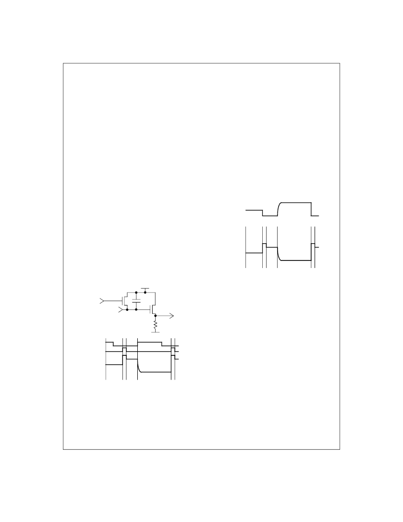
Figure 1 shows the output stage of a typical CCD and the result-
ing output waveform:
Capacitor C1 converts the electrons coming from the CCD’s shift
register to an analog voltage. The source follower output stage
(Q2) buffers this voltage before it leaves the CCD. Q1 resets the
voltage across capacitor C1 in between every pixel at intervals 2
and 5. When Q1 is on, the output signal (OS) is at its most posi-
tive voltage. After Q1 turns off (period 3), the OS level represents
the residual voltage across C1 (V
RESIDUAL
). V
RESIDUAL
includes
charge injection from Q1, thermal noise from the ON resistance
of Q1, and other sources of error. When the shift register clock
(1) makes a low to high transition (period 4), the electrons from
the next pixel flow into C1. The charge across C1 now contains
the voltage proportional to the number of electrons plus V
RESID-
UAL
, an error term. If OS is sampled at the end of period 3 and
that voltage is subtracted from the OS at the end of period 4, the
V
RESIDUAL
term is canceled and the noise on the signal is
reduced ([V
SIGNAL
+V
RESIDUAL
]-V
RESIDUAL
= V
SIGNAL
). This is the
principal of Correlated Double Sampling.
The LM9812’s CDS circuit acquires a signal within a 1 MCLK win-
dow which can be placed anywhere in the pixel period with 0.5
MCLK precision. See Diagram 12 for more detailed timing infor-
mation.
1.2 CIS Mode
The LM9812 provides some support for CIS (Contact Image Sen-
sor) devices by offering a sampling mode for capturing positive
going signals, as opposed to the CCD’s negative going signal.
The output signal of a CIS sensor (Figure 2) differs from a CCD
signal in two primary ways: its output increases with increasing
signal strength, and it does not usually have a reference level as
an integral part of the output waveform of every pixel.
When the LM9812 is in CIS mode (Register 24, bit 7=1), it uses
the V
REF MID
level as the reference (or black) voltage for each
pixel. Since the LM9812 clamps the input signal to V
REF MID
at
the black portion at the beginning of every line, the output of the
sampler is an accurate and repeatable representation of the that
pixel’s brightness.
1.2.1 Static PGAs
The output of the CDS stage drives the PGAs (Programmable
Gain Amplifiers). Each PGA provides 5 bits of fixed gain correc-
tion over a 0.93V/V to 3V/V (-0.6 to 9.5dB) range. The Blue chan-
nel has an optional x3 stage for a gain range of 2.8V/V to 9.0V/V
(8.9 to 19dB). The gain of each PGA should be set during calibra-
tion to bring the maximum amplitude of the strongest pixel to a
level just below the desired maximum output from the ADC. The
gain is determined by the following equation:
Gain V
Equation 1: PGA Gain
The Blue Channel has an additional gain stage with a gain of
3V/V that may be switched on to compensate for the low ampli-
tude blue output of some sensors. With the x3 bit set (Register 2,
bit 7=1), the blue gain is:
Gain V
Equation 2: Blue Channel PGA Gain with x3 Bit Set
RS (RESET)
e-
(from shift register)
OS
Q1
Q2
C1
V
DD
V
SS
1
RS
OS
1
2
3
4
5
Figure 1: CDS
OS (CCD)
1
2
3
4
5
Figure 2: CIS vs. CCD Output signals
OS (CIS)
0.93
PG32
+
=
02.79
PG32
+
=
相關PDF資料 |
PDF描述 |
|---|---|
| LM9823CCWM | LM9823 3 Channel 48-Bit Color Scanner Analog Front End |
| LM9823CCWMX | LM9823 3 Channel 48-Bit Color Scanner Analog Front End |
| LMC13204 | Quad SPST High Voltage CMOS Analog Switches |
| LMC13334 | Quad SPST High Voltage CMOS Analog Switches |
| LMC13335 | Quad SPST High Voltage CMOS Analog Switches |
相關代理商/技術參數(shù) |
參數(shù)描述 |
|---|---|
| LM981-SC36 | 功能描述:基本/快動開關 Foot Switch RoHS:否 制造商:Omron Electronics 觸點形式:SPDT 執(zhí)行器:Lever 電流額定值:5 A 電壓額定值 AC:250 V 電壓額定值 DC:30 V 功率額定值: 工作力:120 g IP 等級:IP 67 NEMA 額定值: 端接類型:Wire 安裝:Panel |
| LM981-ZZ | 功能描述:基本/快動開關 Foot Switch RoHS:否 制造商:Omron Electronics 觸點形式:SPDT 執(zhí)行器:Lever 電流額定值:5 A 電壓額定值 AC:250 V 電壓額定值 DC:30 V 功率額定值: 工作力:120 g IP 等級:IP 67 NEMA 額定值: 端接類型:Wire 安裝:Panel |
| LM981-ZZ-1 | 功能描述:基本/快動開關 Foot Switch RoHS:否 制造商:Omron Electronics 觸點形式:SPDT 執(zhí)行器:Lever 電流額定值:5 A 電壓額定值 AC:250 V 電壓額定值 DC:30 V 功率額定值: 工作力:120 g IP 等級:IP 67 NEMA 額定值: 端接類型:Wire 安裝:Panel |
| LM9820 | 制造商:未知廠家 制造商全稱:未知廠家 功能描述: |
| LM9820CCWM | 制造商:NSC 制造商全稱:National Semiconductor 功能描述:LM9810/20 10/12-Bit Image Sensor Processor Analog Front End |
發(fā)布緊急采購,3分鐘左右您將得到回復。