- 您現(xiàn)在的位置:買賣IC網(wǎng) > PDF目錄299245 > K7A403601A-QC140 128K X 36 CACHE SRAM, 4 ns, PQFP100 PDF資料下載
參數(shù)資料
| 型號(hào): | K7A403601A-QC140 |
| 元件分類: | SRAM |
| 英文描述: | 128K X 36 CACHE SRAM, 4 ns, PQFP100 |
| 封裝: | 20 X 14 MM, TQFP-100 |
| 文件頁(yè)數(shù): | 10/15頁(yè) |
| 文件大小: | 401K |
| 代理商: | K7A403601A-QC140 |
第1頁(yè)第2頁(yè)第3頁(yè)第4頁(yè)第5頁(yè)第6頁(yè)第7頁(yè)第8頁(yè)第9頁(yè)當(dāng)前第10頁(yè)第11頁(yè)第12頁(yè)第13頁(yè)第14頁(yè)第15頁(yè)
K7A403601A
128Kx36 Synchronous SRAM
- 4 -
Rev 1.0
2000
The K7A403601A is a synchronous SRAM designed to support the burst address accessing sequence of the P6 and Power PC
based microprocessor. All inputs (with the exception of
, LBO
of the burst access is controlled by ADSC ADSP and
and chip select pins.
The accesses are enabled with the chip select signals and output enabled signals. Wait states are inserted into the access with
.
When ZZ is pulled high, the SRAM will enter a Power Down State. At this time, internal state of the SRAM is preserved. When ZZ
Read cycles are initiated with ADSP
WEx and
)using the new external address clocked into the on-chip address
register whenever
is sampled low, the chip selects are sampled active, and the output buffer is enabled with OE
ation the data of cell array accessed by the current address, registered in the Data-out registers by the positive edge of CLK, are car-
output
pins.
is ignored on the clock edge that samples ADSP
increases internally for the next access of the burst when WE
ADV is sampled low. And
is blocked to
control signals by disabling
1
.
GW(regaedless of
and WE
BW and
x
when
is high.
Write cycles are performed by disabling the output buffers with
and asserting WE
WEx are ignored on the clock edge that sam-
ADSP low, but are sampled on the subsequent clock edges. The output buffers are disabled when
x are sampled
Low(regaedless of
). Data is clocked into the data input register when WE
next address of burst, if both WE
ADV are sampled Low. Individual byte write cycles are performed by any one or more byte
WEa,
b, WE
WEd) sampled low. The
a control DQa0
7
and DQPa,
b controls DQb0
7
and DQPb, WEc controls DQc ~ DQc7
and
d control DQd0
7
and DQPd. Read or write cycle may also be initi-
ADSC, instead of
. The differences between cycles initiated with ADSC
ADSP as are follows;
ADSP must be sampled high when
is sampled low to initiate a cycle with ADSC
WE
ADSC low(and
high).
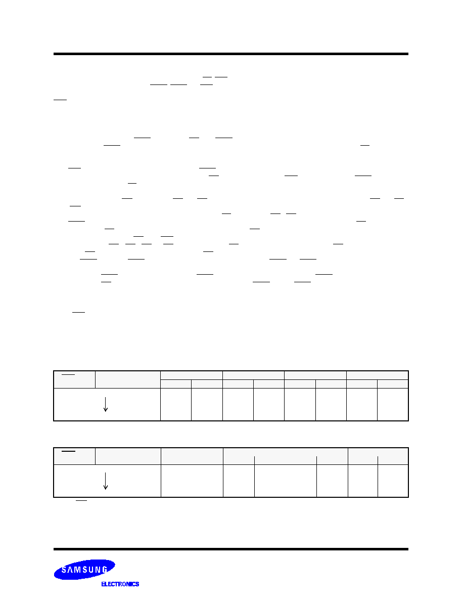
Addresses are generated for the burst access as shown below, The starting point of the burst sequence is provided by the externa
address. The burst address counter wraps around to its initial state upon completion. The burst sequence is determined by the state
LBO pin. When this pin is Low, linear burst sequence is selected. When this pin is High, Interleaved burst sequence is
BURST SEQUENCE TABLE
(Interleaved Burst)
PIN
HIGH
Case 2
Case 3
A1
0
A
A0
1
A
A1
0
First Address
0
1
0
1
0
1
0
1
0
1
0
1
0
1
0
(Linear Burst)
1. LBO
.
LBO
LOW
Case 1
Case 3
Case 4
1
A
A1
0
A
A0
1
A
First Address
Fourth Address
0
1
0
1
0
1
0
1
0
1
0
1
0
相關(guān)PDF資料 |
PDF描述 |
|---|---|
| K85X-AA-15P-K30 | 15 CONTACT(S), MALE, D SUBMINIATURE CONNECTOR, SOLDER, PLUG |
| K85X-AA-15P-KJ15 | 15 CONTACT(S), MALE, D SUBMINIATURE CONNECTOR, SOLDER, PLUG |
| K85X-AA-15P-KJ30 | 15 CONTACT(S), MALE, D SUBMINIATURE CONNECTOR, SOLDER, PLUG |
| K85X-AA-15P-KJ | 15 CONTACT(S), MALE, D SUBMINIATURE CONNECTOR, SOLDER, PLUG |
| K85X-AA-15P-K | 15 CONTACT(S), MALE, D SUBMINIATURE CONNECTOR, SOLDER, PLUG |
相關(guān)代理商/技術(shù)參數(shù) |
參數(shù)描述 |
|---|---|
| K7A403601B | 制造商:SAMSUNG 制造商全稱:Samsung semiconductor 功能描述:128Kx36/x32 & 256Kx18 Synchronous SRAM |
| K7A403601B-QC | 制造商:SAMSUNG 制造商全稱:Samsung semiconductor 功能描述:128Kx36/x32 & 256Kx18 Synchronous SRAM |
| K7A403609A | 制造商:SAMSUNG 制造商全稱:Samsung semiconductor 功能描述:128Kx36 & 256Kx18-Bit Synchronous Pipelined Burst SRAM |
| K7A403609B | 制造商:SAMSUNG 制造商全稱:Samsung semiconductor 功能描述:128Kx36/x32 & 256Kx18 Synchronous SRAM |
| K7A403609B_06 | 制造商:SAMSUNG 制造商全稱:Samsung semiconductor 功能描述:128Kx36/x32 & 256Kx18 Synchronous SRAM |
發(fā)布緊急采購(gòu),3分鐘左右您將得到回復(fù)。