- 您現(xiàn)在的位置:買賣IC網(wǎng) > PDF目錄299245 > K6L0908V2A-TD850 64K X 8 STANDARD SRAM, 85 ns, PDSO32 PDF資料下載
參數(shù)資料
| 型號(hào): | K6L0908V2A-TD850 |
| 元件分類: | SRAM |
| 英文描述: | 64K X 8 STANDARD SRAM, 85 ns, PDSO32 |
| 封裝: | 8 X 20 MM, TSOP1-32 |
| 文件頁數(shù): | 6/10頁 |
| 文件大小: | 193K |
| 代理商: | K6L0908V2A-TD850 |
K6L0908V2A, K6L0908U2A Family
CMOS SRAM
Revision 3.0
February 1998
5
AC CHARACTERISTICS (K6L0908V2B Family:Vcc=3.0~3.6V, K6L0908U2B Family:Vcc=2.7~3.3V,
Commercial product:TA=0 to 70
°C, Extended product:TA=-25 to 85°C, Industrial product:TA=-40 to 85°C)
Parameter List
Symbol
Speed Bins
Units
70ns
85ns
100ns
Min
Max
Min
Max
Min
Max
Read
Read cycle time
tRC
70
-
85
-
100
-
ns
Address access time
tAA
-
70
-
85
-
100
ns
Chip select to output
tCO
-
70
-
85
-
100
ns
Output enable to valid output
tOE
-
35
-
45
-
50
ns
Chip select to low-Z output
tLZ
10
-
10
-
10
-
ns
Output enable to low-Z output
tOLZ
5
-
5
-
5
-
ns
Chip disable to high-Z output
tHZ
0
25
0
30
0
30
ns
Output disable to high-Z output
tOHZ
0
25
0
20
0
20
ns
Output hold from address change
tOH
10
-
10
-
15
-
ns
Write
Write cycle time
tWC
70
-
85
-
100
-
ns
Chip select to end of write
tCW
60
-
70
-
80
-
ns
Address set-up time
tAS
0
-
0
-
0
-
ns
Address valid to end of write
tAW
60
-
70
-
80
-
ns
Write pulse width
tWP
55
-
60
-
70
-
ns
Write recovery time
tWR
0
-
0
-
0
-
ns
Write to output high-Z
tWHZ
0
25
0
25
0
30
ns
Data to write time overlap
tDW
30
-
35
-
40
-
ns
Data hold from write time
tDH
0
-
0
-
0
-
ns
End write to output low-Z
tOW
5
-
5
-
5
-
ns
CL1)
1. Including scope and jig capacitance
AC OPERATING CONDITIONS
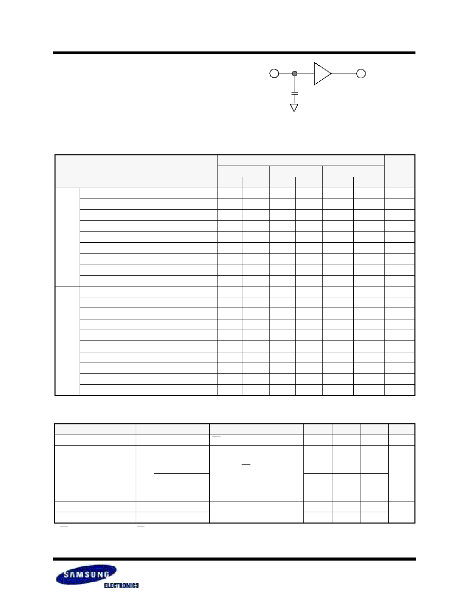
TEST CONDITIONS( Test Load and Input/Output Reference)
Input pulse level : 0.4 to 2.2V
Input rising and falling time : 5ns
Input and output reference voltage :1.5V
Output load(see right) : CL=100pF+1TTL
1)CL=30pF+1TTL
1. K6L0908V2A-70 Family, K6L0908U2A-85 Family
DATA RETENTION CHARACTERISTICS
1. CS1
≥Vcc-0.2V, CS2 ≥Vcc-0.2V( CS1 controlled) or CS2≤0.2V(CS2 controlled)
Item
Symbol
Test Condition
Min
Typ
Max
Unit
Vcc for data retention
VDR
CS11)
≥Vcc-0.2V
2.0
-
3.6
V
Data retention current
IDR
K6L0908V2A-B
K6L0908V2A-D
K6L0908V2A-F
Vcc=3.0V, CS1
≥Vcc-0.2V,
CS2
≥Vcc-0.2V or CS2≤0.2V
-
10
15
A
K6L0908U2A-B
K6L0908U2A-D
K6L0908U2A-F
-
8
10
Data retention set-up time
tSDR
See data retention waveform
0
-
ms
Recovery time
tRDR
5
-
相關(guān)PDF資料 |
PDF描述 |
|---|---|
| K7A163280A-QI16 | 512K X 32 CACHE SRAM, 3.5 ns, PQFP100 |
| K7A403601A-QC140 | 128K X 36 CACHE SRAM, 4 ns, PQFP100 |
| K85X-AA-15P-K30 | 15 CONTACT(S), MALE, D SUBMINIATURE CONNECTOR, SOLDER, PLUG |
| K85X-AA-15P-KJ15 | 15 CONTACT(S), MALE, D SUBMINIATURE CONNECTOR, SOLDER, PLUG |
| K85X-AA-15P-KJ30 | 15 CONTACT(S), MALE, D SUBMINIATURE CONNECTOR, SOLDER, PLUG |
相關(guān)代理商/技術(shù)參數(shù) |
參數(shù)描述 |
|---|---|
| K6LCH | 制造商:ABB Low Voltage Products and Systems 功能描述:LUG COVER, HIGH RCS S6 3P ISO |
| K6MR8MGW10 | 制造商:SUNLED 制造商全稱:SunLED Corporation 功能描述:26mm LED CLUSTER |
| K6PICF | 制造商:Ideal Industries 功能描述:Bulk |
| K6PIDG | 制造商:Ideal Industries Inc 功能描述: |
| K6-PS | 制造商:Panasonic Electric Works 功能描述: |
發(fā)布緊急采購,3分鐘左右您將得到回復(fù)。