- 您現(xiàn)在的位置:買賣IC網(wǎng) > PDF目錄384544 > ISPPAC-CLK55xx (Lattice Semiconductor Corporation) In-System Programmable Clock Generator with Universal Fan-Out Buffer PDF資料下載
參數(shù)資料
| 型號: | ISPPAC-CLK55xx |
| 廠商: | Lattice Semiconductor Corporation |
| 英文描述: | In-System Programmable Clock Generator with Universal Fan-Out Buffer |
| 中文描述: | 在系統(tǒng)可編程時鐘發(fā)生器與通用扇出緩沖器 |
| 文件頁數(shù): | 18/43頁 |
| 文件大小: | 867K |
| 代理商: | ISPPAC-CLK55XX |
第1頁第2頁第3頁第4頁第5頁第6頁第7頁第8頁第9頁第10頁第11頁第12頁第13頁第14頁第15頁第16頁第17頁當(dāng)前第18頁第19頁第20頁第21頁第22頁第23頁第24頁第25頁第26頁第27頁第28頁第29頁第30頁第31頁第32頁第33頁第34頁第35頁第36頁第37頁第38頁第39頁第40頁第41頁第42頁第43頁
Lattice Semiconductor
ispClock5500 Family Data Sheet
18
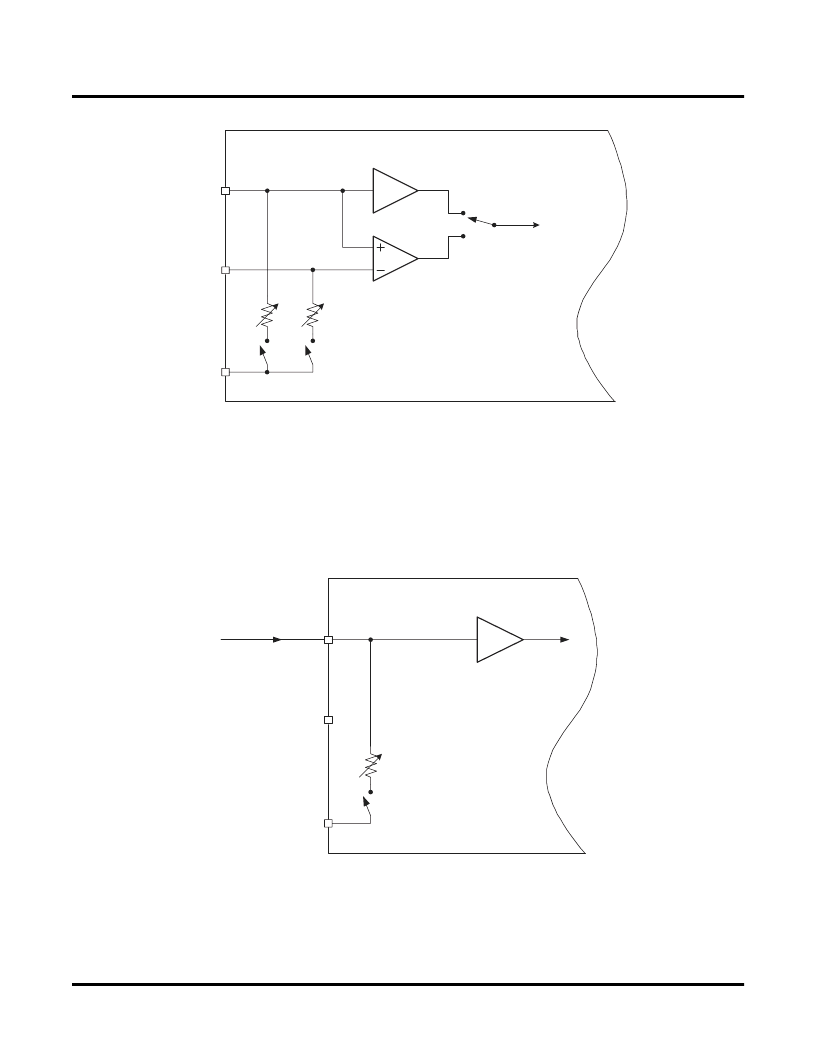
Figure 12. ispClock5500 Clock Reference Input Structure (REFA+/- Pair Shown)
The following usage guidelines are suggested for interfacing to supported logic families.
LVTTL (3.3V), LVCMOS (1.8V, 2.5V, 3.3V)
The receiver should be set to LVCMOS or LVTTL mode, and the input signal should be connected to the ‘+’ termi-
nal of the input pair (e.g. REFA+). The ‘-’ input terminal should be left
fl
oating. CMOS transmission lines are gener-
ally source terminated, so all termination resistors should be set to the OPEN state. Figure 13 shows the proper
con
fi
guration. Please note that because switching thresholds are different for LVCMOS running at 1.8V, there is a
separate con
fi
guration setting for this particular standard.
Figure 13. LVCMOS/LVTTL Input Receiver Configuration
HSTL, SSTL2, SSTL3
The receiver should be set to HSTL/SSTL mode, and the input signal should be fed into the ‘+’ terminal of the input
pair. The ‘-’ input terminal should be tied to the appropriate V
ref
value, and the REFVTT terminal should be tied to a
V
TT
termination supply. The positive input’s terminating resistor should be engaged and set to 50
. Figure 14
shows an appropriate con
fi
guration. Refer to the “Recommended Operating Conditions - Supported Logic Stan-
dards” table in this data sheet for suitable values of V
REF
and V
TT.
R
T
R
T
REFA-
REFA+
REFVTT
To Internal
Logic
Single-ended
Receiver
ispClock5500
Differential
Receiver
R
T
OPEN
REFA-
REFA+
REFVTT
Single-ended
Receiver
No Connect
No Connect
Signal In
ispClock5500
相關(guān)PDF資料 |
PDF描述 |
|---|---|
| ISPPAC-CLK5510V | In-System Programmable Clock Generator with Universal Fan-Out Buffer |
| ISPPAC-CLK5510V-01T48C | In-System Programmable Clock Generator with Universal Fan-Out Buffer |
| ISPPAC-CLK5510V-01T48I | In-System Programmable Clock Generator with Universal Fan-Out Buffer |
| ISPPAC-CLK5520V-01T100C | LED Area Light; LED Color:Blue; Leaded Process Compatible:No; Light Emitting Area:62x62mm; Peak Reflow Compatible (260 C):No; Supply Current:200mA; Supply Voltage:24VDC; Wavelength:470nm |
| ISPPAC-CLK5520V-01T100I | Linear Array Light; LED Color:Blue; Leaded Process Compatible:No; Peak Reflow Compatible (260 C):No; Supply Current:800mA; Supply Voltage:24VDC; Wavelength:470nm |
相關(guān)代理商/技術(shù)參數(shù) |
參數(shù)描述 |
|---|---|
| ISPPACCLK5610AV-01T100C | 制造商:LATTICE 制造商全稱:Lattice Semiconductor 功能描述:In-System Programmable, Enhanced Zero-Delay, Clock Generator with Universal Fan-Out Buffer |
| ISPPACCLK5610AV-01T100I | 制造商:LATTICE 制造商全稱:Lattice Semiconductor 功能描述:In-System Programmable, Enhanced Zero-Delay, Clock Generator with Universal Fan-Out Buffer |
| ispPAC-CLK5610AV-01T48C | 功能描述:時鐘驅(qū)動器及分配 ISP 0 Delay Clock Ge n w/Unv Fan-Out Buf RoHS:否 制造商:Micrel 乘法/除法因子:1:4 輸出類型:Differential 最大輸出頻率:4.2 GHz 電源電壓-最大: 電源電壓-最小:5 V 最大工作溫度:+ 85 C 封裝 / 箱體:SOIC-8 封裝:Reel |
| ISPPACCLK5610AV-01T48C | 制造商:LATTICE 制造商全稱:Lattice Semiconductor 功能描述:In-System Programmable, Enhanced Zero-Delay, Clock Generator with Universal Fan-Out Buffer |
| ispPAC-CLK5610AV-01T48I | 功能描述:時鐘驅(qū)動器及分配 ISP 0 Dlay Clck Gen w/Unv Fan-Out Buf I RoHS:否 制造商:Micrel 乘法/除法因子:1:4 輸出類型:Differential 最大輸出頻率:4.2 GHz 電源電壓-最大: 電源電壓-最小:5 V 最大工作溫度:+ 85 C 封裝 / 箱體:SOIC-8 封裝:Reel |
發(fā)布緊急采購,3分鐘左右您將得到回復(fù)。