- 您現(xiàn)在的位置:買賣IC網(wǎng) > PDF目錄385436 > HYS72T512022HR (QIMONDA) 240-Pin Registered DDR2 SDRAM Modules PDF資料下載
參數(shù)資料
| 型號: | HYS72T512022HR |
| 廠商: | QIMONDA |
| 英文描述: | 240-Pin Registered DDR2 SDRAM Modules |
| 中文描述: | 240針DDR2 SDRAM的注冊模塊 |
| 文件頁數(shù): | 18/41頁 |
| 文件大小: | 1063K |
| 代理商: | HYS72T512022HR |
第1頁第2頁第3頁第4頁第5頁第6頁第7頁第8頁第9頁第10頁第11頁第12頁第13頁第14頁第15頁第16頁第17頁當前第18頁第19頁第20頁第21頁第22頁第23頁第24頁第25頁第26頁第27頁第28頁第29頁第30頁第31頁第32頁第33頁第34頁第35頁第36頁第37頁第38頁第39頁第40頁第41頁

Internet Data Sheet
Rev. 1.2, 2007-01
03292006-AYVF-ZIIJ
18
HYS72T[512/256]02xHR–[3S/3.7/5]–A
Registered DDR2 SDRAM Modules
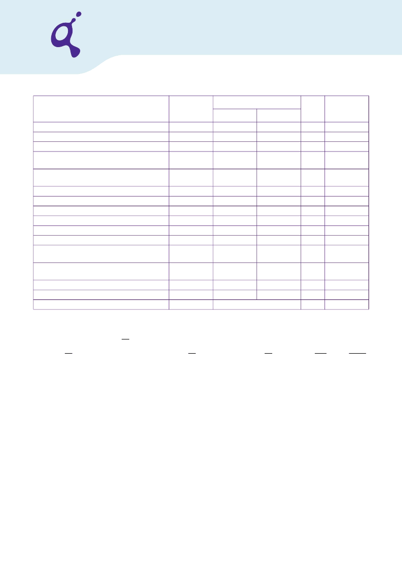
DQ hold skew factor
Read preamble
Read postamble
Active to active command period for 1KB page
size products
Active to active command period for 2KB page
size products
Internal Read to Precharge command delay
Write preamble
Write postamble
Write recovery time
Internal write to read command delay
Exit power down to read command
Exit active power-down mode to read command
(slow exit, lower power)
Exit precharge power-down to any valid
command (other than NOP or Deselect)
Exit self-refresh to a non-read command
Exit self-refresh to read command
Write command to DQS associated clock edges
1) For details and notes see the relevant Qimonda component data sheet
2)
V
DDQ
= 1.8 V ± 0.1V;
V
DD
= 1.8 V ± 0.1 V. See notes
5)6)7)8)
3) Timing that is not specified is illegal and after such an event, in order to guarantee proper operation, the DRAM must be powered down
and then restarted through the specified initialization sequence before normal operation can continue.
4) Timings are guaranteed with CK/CK differential Slew Rate of 2.0 V/ns. For DQS signals timings are guaranteed with a differential Slew
Rate of 2.0 V/ns in differential strobe mode and a Slew Rate of 1 V/ns in single ended mode.
5) The CK / CK input reference level (for timing reference to CK / CK) is the point at which CK and CK cross. The DQS / DQS, RDQS / RDQS,
input reference level is the crosspoint when in differential strobe mode.
6) Inputs are not recognized as valid until
V
REF
stabilizes. During the period before
V
REF
stabilizes, CKE = 0.2 x
V
DDQ
is recognized as low.
7) The output timing reference voltage level is
V
TT
.
8) New units, ‘
t
CK.AVG
‘ and ‘nCK‘, are introduced in DDR2–667 and DDR2–800. Unit ‘
t
CK.AVG
‘ represents the actual
t
CK.AVG
of the input clock
under operation. Unit ‘nCK‘ represents one clock cycle of the input clock, counting the actual clock edges. Note that in DDR2–400 and
DDR2–533, ‘
t
‘ is used for both concepts. Example:
t
= 2 [nCK] means; if Power Down exit is registered at Tm, an Active command
may be registered at Tm + 2, even if (Tm + 2 - Tm) is 2 x
t
CK.AVG
+
t
ERR.2PER(Min)
.
9) When the device is operated with input clock jitter, this parameter needs to be derated by the actual
t
of the input clock. (output
deratings are relative to the SDRAM input clock.) For example, if the measured jitter into a DDR2–667 SDRAM has
t
ERR(6-10PER).MIN
= – 272
ps and
t
ERR(6- 10PER).MAX
= + 293 ps, then
t
DQSCK.MIN(DERATED)
=
t
DQSCK.MIN
–
t
ERR(6-10PER).MAX
= – 400 ps – 293 ps = – 693 ps and
t
=
–
t
= 400 ps + 272 ps = + 672 ps. Similarly,
t
for DDR2–667 derates to
t
LZ.DQ.MIN(DERATED)
= - 900 ps – 293 ps = – 1193 ps and
t
LZ.DQ.MAX(DERATED)
= 450 ps + 272 ps = + 722 ps. (Caution on the MIN/MAX usage!)
10) Input clock jitter spec parameter. These parameters are referred to as 'input clock jitter spec parameters' and these parameters apply to
DDR2–667 and DDR2–800 only. The jitter specified is a random jitter meeting a Gaussian distribution.
11) These parameters are specified per their average values, however it is understood that the relationship between the average timing and
the absolute instantaneous timing holds all the times (min. and max of SPEC values are to be used for calculations ).
12)
t
of 3 clocks means CKE must be registered on three consecutive positive clock edges. CKE must remain at the valid input level the
entire time it takes to achieve the 3 clocks of registration. Thus, after any CKE transition, CKE may not transition from its valid level during
the time period of
t
IS
+ 2 x
t
CK
+
t
IH
.
t
QHS
t
RPRE
t
RPST
t
RRD
—
0.9
0.4
7.5
340
1.1
0.6
—
ps
t
CK.AVG
t
CK.AVG
ns
27)
28)29)
28)30)
31)
t
RRD
10
—
ns
31)
t
RTP
t
WPRE
t
WPST
t
WR
t
WTR
t
XARD
t
XARDS
7.5
0.35
0.4
15
7.5
2
7 – AL
—
—
0.6
—
—
—
—
ns
t
CK.AVG
t
CK.AVG
ns
ns
nCK
nCK
31)
31)
31)32)
t
XP
2
—
nCK
t
XSNR
t
XSRD
WL
t
RFC
+10
200
RL–1
—
—
ns
nCK
nCK
31)
Parameter
Symbol
DDR2–667
Unit
Note
1)2)3)4)5)6)7)8)
Min.
Max.
相關(guān)PDF資料 |
PDF描述 |
|---|---|
| HYS72T512022HR-3.7-A | 240-Pin Registered DDR2 SDRAM Modules |
| HYS72T512022HR-3S-A | 240-Pin Registered DDR2 SDRAM Modules |
| HYS72T512022HR-5-A | 240-Pin Registered DDR2 SDRAM Modules |
| HYS72T256322HP | 240-Pin Dual-Die Registered DDR2 SDRAM Modules |
| HYS72T256322HP-3.7-A | 240-Pin Dual-Die Registered DDR2 SDRAM Modules |
相關(guān)代理商/技術(shù)參數(shù) |
參數(shù)描述 |
|---|---|
| HYS72T512022HR-3.7-A | 制造商:QIMONDA 制造商全稱:QIMONDA 功能描述:240-Pin Registered DDR2 SDRAM Modules |
| HYS72T512022HR-3S-A | 制造商:QIMONDA 制造商全稱:QIMONDA 功能描述:240-Pin Registered DDR2 SDRAM Modules |
| HYS72T512022HR-5-A | 制造商:QIMONDA 制造商全稱:QIMONDA 功能描述:240-Pin Registered DDR2 SDRAM Modules |
| HYS72T512122HFN-3.7-A | 制造商:QIMONDA 制造商全稱:QIMONDA 功能描述:240-Pin Fully-Buffered DDR2 SDRAM Modules DDR2 SDRAM |
| HYS72T512341HHP | 制造商:QIMONDA 制造商全稱:QIMONDA 功能描述:240-Pin Registered DDR2 SDRAM Modules |
發(fā)布緊急采購,3分鐘左右您將得到回復。