- 您現(xiàn)在的位置:買賣IC網(wǎng) > PDF目錄385433 > HYMP112S64MP8-E3 (HYNIX SEMICONDUCTOR INC) SCREW LOCKS MALE PDF資料下載
參數(shù)資料
| 型號(hào): | HYMP112S64MP8-E3 |
| 廠商: | HYNIX SEMICONDUCTOR INC |
| 元件分類: | DRAM |
| 英文描述: | SCREW LOCKS MALE |
| 中文描述: | 128M X 64 DDR DRAM MODULE, 0.6 ns, ZMA200 |
| 封裝: | ROHS COMPLIANT, DIMM-200 |
| 文件頁數(shù): | 11/17頁 |
| 文件大?。?/td> | 405K |
| 代理商: | HYMP112S64MP8-E3 |

HYMP112S64(L)MP8
Rev. 0.1/ July 2004
11
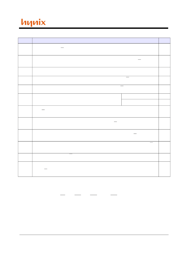
IDD Meauarement Conditions
Note:
1. IDD specifications are tested after the device is properly initialized
2. Input slew rate is specified by AC Parametric Test Condition
3. IDD parameters are specified with ODT disabled.
4. Data bus consists of DQ, DM, DQS, DQS, RDQS, RDQS, LDQS, LDQS, UDQS, and UDQS. IDD values must be met with all combinations
of EMRS bits 10 and 11.
5. Definitions for IDD
LOW is defined as Vin
≤
VILAC(max)
HIGH is defined as Vin
≥
VIHAC(min)
STABLE is defined as inputs stable at a HIGH or LOW level
FLOATING is defined as inputs at VREF = VDDQ/2
SWITCHING is defined as:
inputs changing between HIGH and LOW every other clock cycle (once per two clocks) for address and control signals, and
inputs changing between HIGH and LOW every other data transfer (once per clock) for DQ signals not including masks or strobes.
Symbol
Conditions
Units
IDD0
Operating one bank active-precharge current
; tCK = tCK(IDD), tRC = tRC(IDD), tRAS = tRAS-
min(IDD);CKE is HIGH, CS is HIGH between valid commands;Address bus inputs are SWITCHING;Data bus
inputs are SWITCHING
mA
IDD1
Operating one bank active-read-precharge curren
; IOUT = 0mA;BL = 4, CL = CL(IDD), AL = 0;
tCK = tCK(IDD), tRC = tRC (IDD), tRAS = tRASmin(IDD), tRCD = tRCD(IDD) ; CKE is HIGH, CS is HIGH
between valid commands ; Address bus inputs are SWITCHING ; Data pattern is same as IDD4W
mA
IDD2P
Precharge power-down current
; All banks idle ; tCK = tCK(IDD) ; CKE is LOW ; Other control and address
bus inputs are STABLE; Data bus inputs are FLOATING
mA
IDD2Q
Precharge quiet standby current
;All banks idle; tCK = tCK(IDD);CKE is HIGH, CS is HIGH; Other control
and address bus inputs are STABLE; Data bus inputs are FLOATING
mA
IDD2N
Precharge standby current
; All banks idle; tCK = tCK(IDD); CKE is HIGH, CS is HIGH; Other control and
address bus inputs are SWITCHING; Data bus inputs are SWITCHING
mA
IDD3P
Active power-down current
; All banks open; tCK = tCK(IDD); CKE is
LOW; Other control and address bus inputs are STABLE; Data bus inputs are
FLOATING
Fast PDN Exit MRS(12) = 0
mA
Slow PDN Exit MRS(12) = 1
mA
IDD3N
Active standby current
; All banks open; tCK = tCK(IDD), tRAS = tRASmax(IDD), tRP =tRP(IDD); CKE is
HIGH, CS is HIGH between valid commands; Other control and address bus inputs are SWITCHING; Data bus
inputs are SWITCHING
mA
IDD4W
Operating burst write current
; All banks open, Continuous burst writes; BL = 4, CL = CL(IDD), AL = 0;
tCK = tCK(IDD), tRAS = tRASmax(IDD), tRP = tRP(IDD); CKE is HIGH, CS is HIGH between valid commands;
Address bus inputs are SWITCHING; Data bus inputs are SWITCHING
mA
IDD4R
Operating burst read current
; All banks open, Continuous burst reads, IOUT = 0mA; BL = 4, CL =
CL(IDD), AL = 0; tCK = tCK(IDD), tRAS = tRASmax(IDD), tRP = tRP(IDD); CKE is HIGH, CS is HIGH between
valid commands; Address bus inputs are SWITCHING;; Data pattern is same as IDD4W
mA
IDD5B
Burst refresh current
; tCK = tCK(IDD); Refresh command at every tRFC(IDD) interval; CKE is HIGH, CS is
HIGH between valid commands; Other control and address bus inputs are SWITCHING; Data bus inputs are
SWITCHING
mA
IDD6
Self refresh current
; CK and CK at 0V; CKE £ 0.2V; Other control and address bus inputs are FLOATING;
Data bus inputs are FLOATING
mA
IDD7
Operating bank interleave read current
; All bank interleaving reads, IOUT = 0mA; BL = 4, CL = CL(IDD),
AL = tRCD(IDD)-1*tCK(IDD); tCK = tCK(IDD), tRC = tRC(IDD), tRRD = tRRD(IDD), tRCD = 1*tCK(IDD); CKE
is HIGH, CS is HIGH between valid commands; Address bus inputs are STABLE during DESELECTs; Data pat-
tern is same as IDD4R; - Refer to the following page for detailed timing conditions
mA
相關(guān)PDF資料 |
PDF描述 |
|---|---|
| HYMP112S64MP8-E4 | SCREW LOCKS FEMALE SETS |
| HYS72D64300HBR-5-C | 184-Pin Registered Double Data Rate SDRAM Module |
| HYS72D64300HBR-6-C | 184-Pin Registered Double Data Rate SDRAM Module |
| HYS72D64300HBR-7-C | 184-Pin Registered Double Data Rate SDRAM Module |
| HYS72D64320 | 184-Pin Registered Double Data Rate SDRAM Module |
相關(guān)代理商/技術(shù)參數(shù) |
參數(shù)描述 |
|---|---|
| HYMP112S64MP8-E4 | 制造商:HYNIX 制造商全稱:Hynix Semiconductor 功能描述:DDR2 SDRAM SO-DIMM |
| HYMP112U64CP8-C4 | 制造商:HYNIX 制造商全稱:Hynix Semiconductor 功能描述:240pin DDR2 SDRAM Unbuffered DIMMs |
| HYMP112U64CP8-S5 | 制造商:HYNIX 制造商全稱:Hynix Semiconductor 功能描述:240pin DDR2 SDRAM Unbuffered DIMMs |
| HYMP112U64CP8-S6 | 制造商:HYNIX 制造商全稱:Hynix Semiconductor 功能描述:240pin DDR2 SDRAM Unbuffered DIMMs |
| HYMP112U64CP8-Y5 | 制造商:HYNIX 制造商全稱:Hynix Semiconductor 功能描述:240pin DDR2 SDRAM Unbuffered DIMMs |
發(fā)布緊急采購,3分鐘左右您將得到回復(fù)。