- 您現(xiàn)在的位置:買賣IC網(wǎng) > PDF目錄384416 > HI-8482DT (HOLT INTEGRATED CIRCUITS INC) 384 MCELL 3 VOLT ZERO POWER ISP CPLD - NOT RECOMMENDED for NEW DESIGN PDF資料下載
參數(shù)資料
| 型號: | HI-8482DT |
| 廠商: | HOLT INTEGRATED CIRCUITS INC |
| 元件分類: | 通用總線功能 |
| 英文描述: | 384 MCELL 3 VOLT ZERO POWER ISP CPLD - NOT RECOMMENDED for NEW DESIGN |
| 中文描述: | DUAL LINE RECEIVER, CDIP20 |
| 封裝: | CERDIP-20 |
| 文件頁數(shù): | 2/10頁 |
| 文件大?。?/td> | 676K |
| 代理商: | HI-8482DT |
DIFF
AMP
TESTA
TESTB
INA
CAPA
INB
CAPB
Comp
LEVEL
SHIFT
LEVEL
SHIFT
Comparators
w / hysteresis
Comp
Detect
Level
Detect
Level
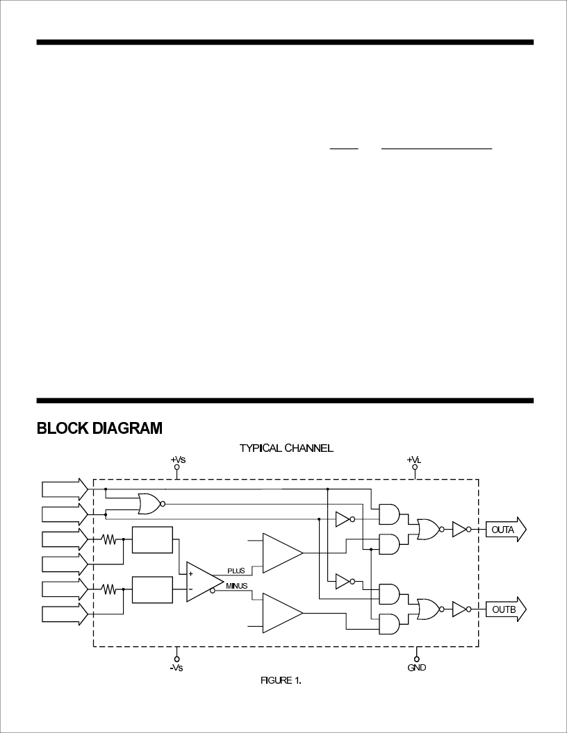
FUNCTIONAL DESCRIPTION
The HI-8482 contains two independent ARINC 429 receive
channels. The diagram in Figure 1 illustrates a typical HI-
8482receivechannel.
ThedifferentialARINCsignalinputisconvertedtoapositive
signal referenced to ground through level shifters and a
unitygaindifferentialamplifier.
A positive differential input signal is converted to a positive
signal on the plus output of the differential amplifier. This
output is proportional in amplitude to the original input
signal. At the same time, the corresponding MINUS output
is pulled to GND. Likewise when a negative input signal is
present at the ARINC inputs, a positive signal is present on
theMINUSoutputandthePLUSoutputispulledtoGND.
The outputs of the differential amplifier are compared with
the ONE, ZERO and NULL threshold levels to produce the
appropriate logic level on the OUTA and OUTB outputs of
the device.
The ARINC clock signal may be recovered
throughaNORfunctionofOUTAandOUTB.
The test inputs logically disconnect the outputs of the
comparators from OUTA and OUTB and force the device
outputs to one of the three valid states (Figure 5).
alleviates having to ground the ARINC inputs during test
modeoperation.
This
ARINC LEVELS
The ARINC 429 specification requires the following
detection levels:
ONE
NULL
ZERO
+6.5V to +13V
+2.5V to -2.5V
-6.5V to -13V
The HI-8482 guarantees recognition of these levels with a
common mode voltage with respect to GND less than
±5V for the worst case condition.
STATE
DIFFERENTIAL VOLTAGE
NOISE
The input hysteresis is set to reject voltage leveltransitions
in the undefined region between the maximum ZERO level
and the minimum NULL level and the undefined region
between the maximum NULL level and the minimum ONE
level.
Therefore, once a valid input differential voltage
thresholdisdetected,theoutputswillremainatavalidlogic
stateuntilanewvalidinputvoltageisdetected.
Inadditiontothehysteresis,theCapAandCapBpinsmake
itpossibletoaddsimpleRCfilterstotheARINCinputs.
HI-8482
HOLT INTEGRATED CIRCUITS
2
相關PDF資料 |
PDF描述 |
|---|---|
| HI-8482J | 384 MCELL 3 VOLT ZERO POWER ISP CPLD - NOT RECOMMENDED for NEW DESIGN |
| HI-8482PSI | ARINC 429 DUAL LINE RECEIVER |
| HI-8482PST | ARINC 429 DUAL LINE RECEIVER |
| HI-8482S | 384 MCELL 3 VOLT ZERO POWER ISP CPLD - NOT RECOMMENDED for NEW DESIGN |
| HI-8482ST | 384 MCELL 3 VOLT ZERO POWER ISP CPLD - NOT RECOMMENDED for NEW DESIGN |
相關代理商/技術參數(shù) |
參數(shù)描述 |
|---|---|
| HI8482J | 制造商:Holt Integrated Circuits 功能描述:Line Receiver 2RX 20-Pin PLCC |
| HI-8482J | 制造商:Holt Integrated Circuits 功能描述:Line Receiver 2RX 20-Pin PLCC |
| HI-8482JF | 制造商:HOLTIC 制造商全稱:Holt Integrated Circuits 功能描述:ARINC 429 DUAL LINE RECEIVER |
| HI-8482JI | 制造商:HOLTIC 制造商全稱:Holt Integrated Circuits 功能描述:ARINC 429 DUAL LINE RECEIVER |
| HI-8482JIF | 制造商:HOLTIC 制造商全稱:Holt Integrated Circuits 功能描述:ARINC 429 DUAL LINE RECEIVER |
發(fā)布緊急采購,3分鐘左右您將得到回復。