- 您現(xiàn)在的位置:買賣IC網(wǎng) > PDF目錄384398 > HE84G762B (King Billion Electronics Co., Ltd.) 8-BIT MICRO-CONTROLLER PDF資料下載
參數(shù)資料
| 型號(hào): | HE84G762B |
| 廠商: | King Billion Electronics Co., Ltd. |
| 英文描述: | 8-BIT MICRO-CONTROLLER |
| 中文描述: | 8位微控制器 |
| 文件頁(yè)數(shù): | 5/60頁(yè) |
| 文件大?。?/td> | 594K |
| 代理商: | HE84G762B |
第1頁(yè)第2頁(yè)第3頁(yè)第4頁(yè)當(dāng)前第5頁(yè)第6頁(yè)第7頁(yè)第8頁(yè)第9頁(yè)第10頁(yè)第11頁(yè)第12頁(yè)第13頁(yè)第14頁(yè)第15頁(yè)第16頁(yè)第17頁(yè)第18頁(yè)第19頁(yè)第20頁(yè)第21頁(yè)第22頁(yè)第23頁(yè)第24頁(yè)第25頁(yè)第26頁(yè)第27頁(yè)第28頁(yè)第29頁(yè)第30頁(yè)第31頁(yè)第32頁(yè)第33頁(yè)第34頁(yè)第35頁(yè)第36頁(yè)第37頁(yè)第38頁(yè)第39頁(yè)第40頁(yè)第41頁(yè)第42頁(yè)第43頁(yè)第44頁(yè)第45頁(yè)第46頁(yè)第47頁(yè)第48頁(yè)第49頁(yè)第50頁(yè)第51頁(yè)第52頁(yè)第53頁(yè)第54頁(yè)第55頁(yè)第56頁(yè)第57頁(yè)第58頁(yè)第59頁(yè)第60頁(yè)

KING BILLION ELECTRONICS CO., LTD
駿
億
電
子
股
份
有
限
公
司
HE84G762B
HE80004 Series
June 1, 2004
This specification is subject to change without notice. Please contact sales person for the latest version before use.
5
V0.92
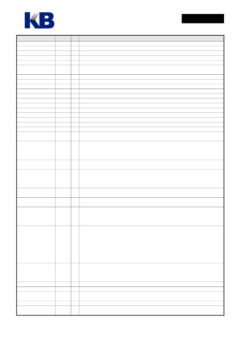
Pin Name
LCAP2B
LCAP2A
LCAP1A
LCAP1B
LCAP3A
Pin # I/O
53
54
55
56
57
Description
O Charge Pump Capacitor Pin.
O Charge Pump Capacitor Pin.
O Charge Pump Capacitor Pin.
O Charge Pump Capacitor Pin.
O Charge Pump Capacitor Pin.
O pumped to LVP. Adjust resistor between LGS1 and LVREG to set LVREG voltage.
I Regulator Voltage Setting
O Reference Voltage Output. Fixed 0.9 Volt DC reference voltage
P Power supply for LCD charge-pump.
P LCD power system ground.
O LCD frame signal for interfacing with LCD segment extender KD80.
O LCD data load pin for interfacing with LCD segment extender KD80.
P Power ground Input.
O Output of OP Amp.
I Non-inverting input of OP Amp.
I Inverting input of OP Amp.
O Alternate output of DAC.
O DAC Output.
System Reset input pin. Level trigger, active low on this pin will put the chip in reset
state.
External fast clock pin. Two types of oscillator can be selected by MO_FXTAL (‘0’ for
RC type and ‘1’ for crystal type). For RC type oscillator, one resistor needs to be
connected between FXI and GND. For crystal oscillator, one crystal needs to be placed
between FXI and FXO. Please refer to application circuit for details.
Test input pin. Please bond this pad and reserve a test point on PCB for debugging. But
for improving ESD, please connect this point with zero Ohm resistor to GND.
External slow clock pins. Slow clock is clock source for LCD display, TIMER1,
Time-Base and other internal blocks. Both crystal and RC oscillator are provided. The
slow clock type can be selected by mask option MO_SXTAL. Choose ‘0’ for RC type
and ‘1’ for crystal oscillator.
Input pin for x32 PLL circuit. Connect to external resistor and capacitors as shown in
application circuit.
P VDD and GND pads as possible for best decoupling effect.
8-bit bi-directional I/O port 10. The output type of I/O pad can also be selected by mask
option MO_10PP[7..0] (‘1’ for push-pull and ‘0’ for open-drain).
As the output structure of I/O pad does not contain tri-state buffer. When using the I/O
pad as input pad, “1” must be outputted before reading.
8-bit bi-directional I/O port D. The output type of I/O pad can also be selected by mask
option MO_DPP[7..0] (‘1’ for push-pull and ‘0’ for open-drain).
As the output structure of I/O pad does not contain tri-state buffer. When using the I/O
as input, ‘1’ must be outputted before reading the pin.
PRTD[7..2] can be used as wake-up pins. PRTD[7..6] can be as external interrupt
sources.
PRTD[1] shares pad with UART Receiver SIN pin.
PRTD[0] shares pad with UART transmitter SOUT pin.
8-bit bi-directional I/O port C. The output type of I/O pad can also be selected by mask
option MO_CPP[7..0] (‘1’ for push-pull and ‘0’ for open-drain).
As the output structure of I/O pad does not contain tri-state buffer. When using the I/O
as input, ‘1’ must be outputted before reading the pin.
P Dedicated power input for RAM
O The Infrared output.
O The PWM output can drive speaker or buzzer directly. Using VDD & PWM to drive
output device.
P Dedicated Ground for PWM output.
107~154 O COM[32..79] pads are shared with SEG[95..48] outputs. The functions of the pads to be
COM drivers or SEG drivers can be selected by mask option MO_COM[1..0]. Please
LVREG
58
LGS1
LVAG
VDD_LCD(VDDA)
GND_LCD(VSSA)
OAC
OCCK
GND
OPO
OPIP
OPIN
DAO
VO
59
60
61
62
63
64
65
66
67
68
69
70
RSTP_N
71
I
FXO,
FXI
72,
73
O,
B
TSTP_P
74
I
SXO,
SXI
75,
76
O,
I
VX
77
I
VDD
78
PRT10[7..0]
79~86
B
PRTD[7..2]
PRTD[1]/SIN
PRTD[0]/SOUT
87~94
B
PRTC[7:0]
95~102 B
VDD_RAM
IRO
103
104
PWM
105
GND_PWM
106
CMSG[32..79]
相關(guān)PDF資料 |
PDF描述 |
|---|---|
| HE84G763B | 8-BIT MICRO-CONTROLLER |
| HE84G770B | 8-BIT MICRO-CONTROLLER |
| HE85750 | 8-bit Micro-controller |
| HE89410 | 8-BIT MICRO-CONTROLLER |
| HE89810 | 8-BIT MICRO-CONTROLLER |
相關(guān)代理商/技術(shù)參數(shù) |
參數(shù)描述 |
|---|---|
| HE84G763(S) | 制造商:未知廠家 制造商全稱:未知廠家 功能描述: |
| HE84G763B | 制造商:KB 制造商全稱:KB 功能描述:8-BIT MICRO-CONTROLLER |
| HE84G770(S) | 制造商:未知廠家 制造商全稱:未知廠家 功能描述: |
| HE84G770B | 制造商:KB 制造商全稱:KB 功能描述:8-BIT MICRO-CONTROLLER |
| HE850 | 制造商:HVPSI 制造商全稱:High Voltage Power Solutions, Inc. 功能描述:SECONDARY SURGE "LIGHTNING" ARRESTER |
發(fā)布緊急采購(gòu),3分鐘左右您將得到回復(fù)。