- 您現(xiàn)在的位置:買賣IC網(wǎng) > PDF目錄375798 > FIN12ACGFX (FAIRCHILD SEMICONDUCTOR CORP) Low Voltage 12-Bit Bi-Directional Serializer/Deserializer with Multiple Frequency Ranges (Preliminary) PDF資料下載
參數(shù)資料
| 型號: | FIN12ACGFX |
| 廠商: | FAIRCHILD SEMICONDUCTOR CORP |
| 元件分類: | 通用總線功能 |
| 英文描述: | Low Voltage 12-Bit Bi-Directional Serializer/Deserializer with Multiple Frequency Ranges (Preliminary) |
| 中文描述: | LINE TRANSCEIVER, PBGA42 |
| 封裝: | 3.50 MM, LEAD FREE, MO-195, BGA-42 |
| 文件頁數(shù): | 3/21頁 |
| 文件大小: | 1819K |
| 代理商: | FIN12ACGFX |
Preliminary
3
www.fairchildsemi.com
F
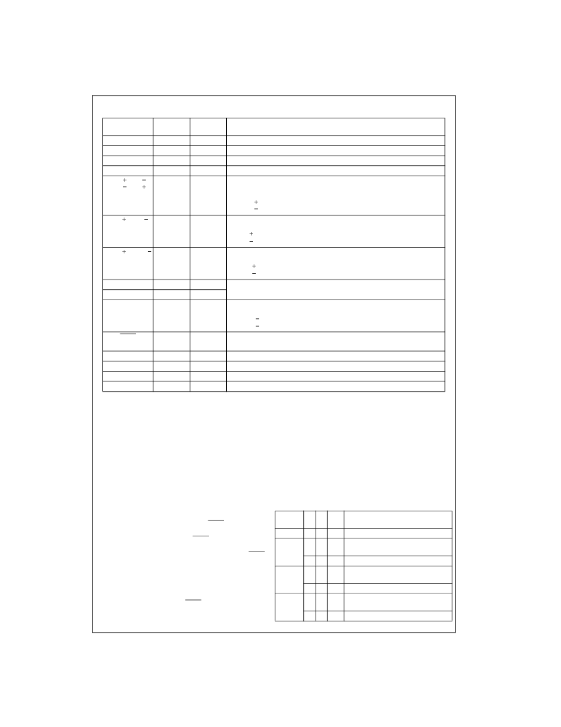
Pin Description
Note 1:
The DSO/DSI serial port terminals have been arranged such that when one device is rotated 180 degrees with respect to the other device the serial
connections will properly align without the need for any traces or cable signals to cross. Other layout orientations may require that traces or cables cross.
Control Logic Circuitry
The FIN12AC has the ability to be used as a 12-bit Serial-
izer or a 12-bit Deserializer. Terminals S1 and S2 must be
set to accommodate the clock reference input frequency
range of the serializer. The table below shows the terminal
programming of these options based on the S1 and S2
control terminals. The DIRI terminal controls whether the
device is the serializer or a deserializer. When DIRI is
asserted LOW, the device is configured as a deserializer.
When the DIRI terminal is asserted HIGH, the device will
be configured as a serializer. Changing the state on the
DIRI signal will reverse the direction of the I/O signals and
generate the opposite state signal on DIRO. For unidirec-
tional operation the DIRI terminal should be hardwired to
the HIGH or LOW state and the DIRO terminal should be
left floating. For bi-directional operation the DIRI of the
master device will be driven by the system and the DIRO
signal of the master will be used to drive the DIRI of the
slave device.
Turn-Around Functionality
The device passes and inverts the DIRI signal through the
device asynchronously to the DIRO signal. Care must be
taken by the system designer to insure that no contention
occurs between the deserializer outputs and the other
devices on this port. Optimally the peripheral device driving
the serializer should be put into a HIGH Impedance state
prior to the DIRI signal being asserted.
When a device with dedicated data outputs turns from a
deserializer to a serializer the dedicated outputs will remain
at the last logical value asserted. This value will only
change if the device is once again turned around into a
deserializer and the values are overwritten.
TABLE 1. Control Logic Circuitry
Pin Name
I/O Type
Number
of Pins
12
1
1
1
2
Description of Signals
DP[1:12]
CKREF
STROBE
CKP
DSO / DSI
DSO / DSI
I/O
IN
IN
OUT
DIFF-I/O
LVCMOS Parallel I/O. Direction controlled by DIRI terminal.
LVCMOS Clock Input and PLL Reference
LVCMOS Strobe Signal for Latching Data into the Serializer
LVCMOS Word Clock Output
CTL Differential Serial I/O Data Signals (Note )
DSO: Refers to output signal pair
DSI: Refers to input signal pair
DSO(I) : Positive signal of DSO(I) pair
DSO(I) : Negative signal of DSO(I) pair
CTL Differential Deserializer Input Bit Clock
CKSI: Refers to signal pair
CKSI : Positive signal of CKSI pair
CKSI : Negative signal of CKSI pair
CTL Differential Serializer Output Bit Clock
CKSO: Refers to signal pair
CKSO : Positive signal of CKSO pair
CKSO : Negative signal of CKSO pair
LVCMOS Mode Selection terminals used to define
frequency range for the RefClock, CKREF
LVCMOS Control Input
Used to control direction of Data Flow:
DIRI
“
1
”
Serializer,
DIRI
“
0
”
Deserializer
CKSI , SKSI
DIFF-IN
2
CKSO , CKSO
DIFF-OUT
2
S1
S2
DIRI
IN
IN
IN
1
1
1
DIRO
OUT
1
LVCMOS Control Output
Inversion of DIRI
Power Supply for Parallel I/O and Translation Circuitry
Power Supply for Core and Serial I/O
Power Supply for Analog PPL Circuitry
Use Bottom Ground Plane for Ground Signals
V
DDP
V
DDS
V
DDA
GND
Supply
Supply
Supply
Supply
1
1
1
0
Mode
0
0
1
0
Description
0
1
X
1
Power-Down Mode
12-Bit Serializer,
20MHz to 56MHz CKREF
12-Bit Deserializer
12-Bit Serializer,
5MHz to 15MHz CKREF
12-Bit Deserializer
12-Bit Serializer,
10MHz to 30MHz CKREF
12-Bit Deserializer
0
1
1
0
0
1
2
1
1
0
1
0
1
3
1
1
0
相關(guān)PDF資料 |
PDF描述 |
|---|---|
| FIN12AC | Low Voltage 12-Bit Bi-Directional Serializer/Deserializer with Multiple Frequency Ranges (Preliminary) |
| FIN12ACMLX | Low Voltage 12-Bit Bi-Directional Serializer/Deserializer with Multiple Frequency Ranges (Preliminary) |
| FIN1531M | 5V LVDS 4-Bit High Speed Differential Driver |
| FIN1531MTC | 5V LVDS 4-Bit High Speed Differential Driver |
| FIN1531MTCX | LINE DRIVER|4 DRIVER|CMOS|TSSOP|16PIN|PLASTIC |
相關(guān)代理商/技術(shù)參數(shù) |
參數(shù)描述 |
|---|---|
| FIN12ACMLX | 功能描述:LVDS 接口集成電路 INTERFACE RoHS:否 制造商:Texas Instruments 激勵器數(shù)量:4 接收機數(shù)量:4 數(shù)據(jù)速率:155.5 Mbps 工作電源電壓:5 V 最大功率耗散:1025 mW 最大工作溫度:+ 85 C 封裝 / 箱體:SOIC-16 Narrow 封裝:Reel |
| FIN12Y WAF | 制造商:Fairchild Semiconductor Corporation 功能描述: |
| FIN1531 | 制造商:FAIRCHILD 制造商全稱:Fairchild Semiconductor 功能描述:5V LVDS 4-Bit High Speed Differential Driver |
| FIN1531M | 功能描述:LVDS 接口集成電路 5V Hi Speed Driver LVDS 4Bit Differ RoHS:否 制造商:Texas Instruments 激勵器數(shù)量:4 接收機數(shù)量:4 數(shù)據(jù)速率:155.5 Mbps 工作電源電壓:5 V 最大功率耗散:1025 mW 最大工作溫度:+ 85 C 封裝 / 箱體:SOIC-16 Narrow 封裝:Reel |
| FIN1531M_Q | 功能描述:LVDS 接口集成電路 5V Hi Speed Driver LVDS 4Bit Differ RoHS:否 制造商:Texas Instruments 激勵器數(shù)量:4 接收機數(shù)量:4 數(shù)據(jù)速率:155.5 Mbps 工作電源電壓:5 V 最大功率耗散:1025 mW 最大工作溫度:+ 85 C 封裝 / 箱體:SOIC-16 Narrow 封裝:Reel |
發(fā)布緊急采購,3分鐘左右您將得到回復。