- 您現(xiàn)在的位置:買賣IC網 > PDF目錄17036 > EVAL-AD7843EBZ (Analog Devices Inc)BOARD EVAL FOR AD7843 PDF資料下載
參數(shù)資料
| 型號: | EVAL-AD7843EBZ |
| 廠商: | Analog Devices Inc |
| 文件頁數(shù): | 4/21頁 |
| 文件大小: | 0K |
| 描述: | BOARD EVAL FOR AD7843 |
| 標準包裝: | 1 |
| ADC 的數(shù)量: | 1 |
| 位數(shù): | 12 |
| 采樣率(每秒): | 125k |
| 數(shù)據接口: | 串行 |
| 輸入范圍: | 0 ~ 5.25 V |
| 在以下條件下的電源(標準): | 1.4mW @ 125kSPS |
| 工作溫度: | -40°C ~ 85°C |
| 已用 IC / 零件: | AD7843 |
| 已供物品: | 板 |
| 相關產品: | AD7843ARUZ-ND - IC ADC 12BIT TOUCHSCREEN 16TSSOP AD7843ARUZ-REEL7-ND - IC ADC 12BIT TOUCHSCREEN 16TSSOP AD7843ARQZ-ND - IC ADC 12BIT TOUCHSCREEN 16-QSOP AD7843ARQZ-REEL7-ND - IC ADC 12BIT TOUCHSCREEN 16-QSOP AD7843ARQZ-REEL-ND - IC ADC 12BIT TOUCHSCREEN 16-QSOP |
AD7843
Rev. B | Page 11 of 20
CIRCUIT INFORMATION
The AD7843 is a fast, low-power, 12-bit, single-supply, A/D
converter. The AD7843 can be operated from a 2.2 V to 5.25 V
supply. When operated from either a 5 V supply or a 3 V supply,
the AD7843 is capable of throughput rates of 125 kSPS when
provided with a 2 MHz clock.
The AD7843 provides the user with an on-chip track-and-hold,
multiplexer, ADC, and serial interface housed in tiny 16-lead
QSOP or TSSOP packages, which offer the user considerable
space-saving advantages over alternative solutions. The serial
clock input (DCLK) accesses data from the part and also provides
the clock source for the successive approximation ADC. The
analog input range is 0 V to VREF (where the externally-applied
VREF can be between 1 V and VCC).
The analog input to the ADC is provided via an on-chip
multiplexer. This analog input can be any one of the X and Y
panel coordinates. The multiplexer is configured with low
resistance switches that allow an unselected ADC input channel
to provide power and an accompanying pin to provide ground
for an external device. For some measurements, the on resistance
of the switches could present a source of error. However, with a
differential input to the converter and a differential reference
architecture, this error can be negated.
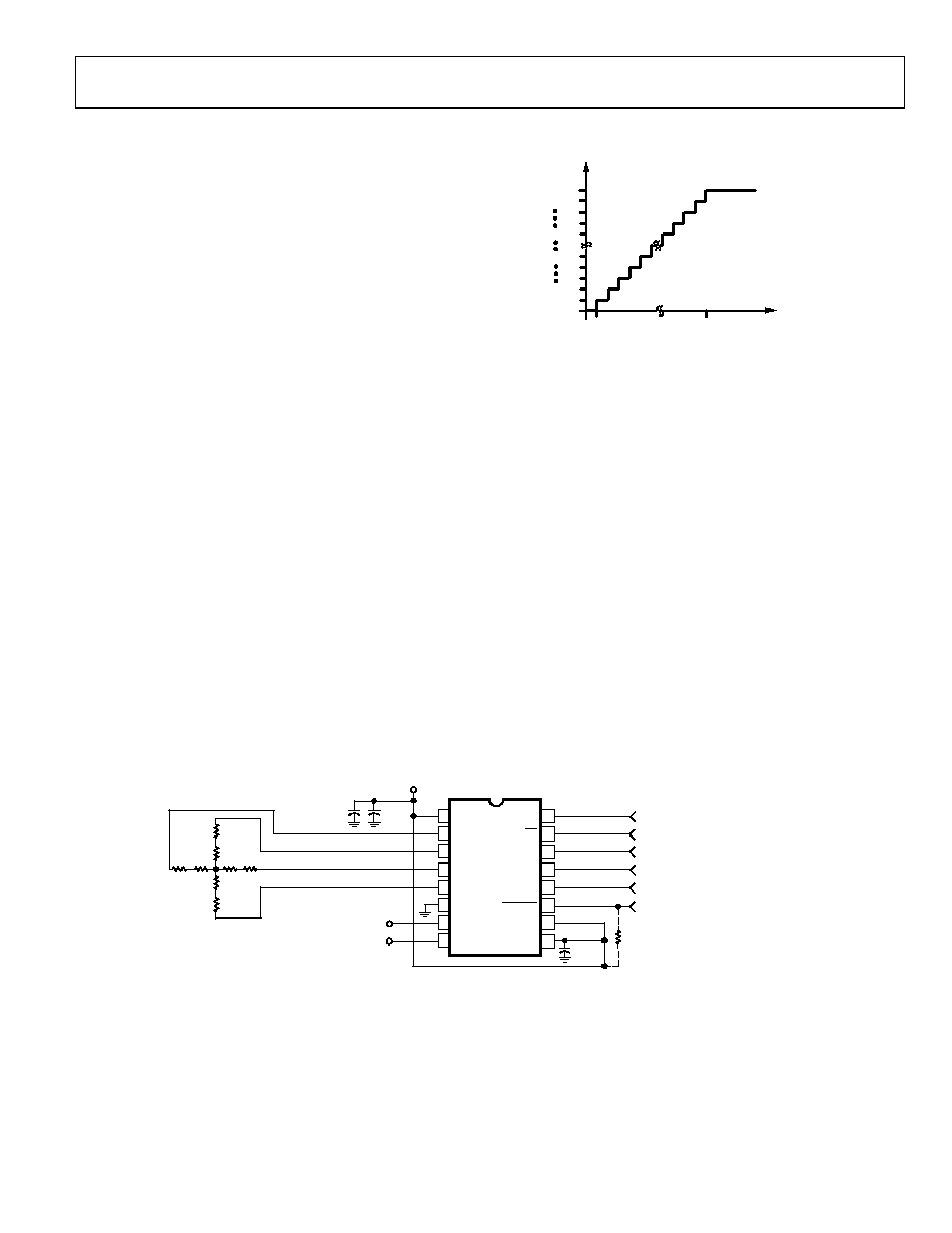
ADC TRANSFER FUNCTION
The output coding of the AD7843 is straight binary. The
designed code transitions occur at successive integer LSB values
(that is, 1 LSB, 2 LSBs, and so forth.). The LSB size equals
VREF/4096. The ideal transfer characteristic for the AD7843 is
shown in Figure 17.
02144-B
-017
ADC
CODE
ANALOG INPUT
1LSB
0V
+VREF–1LSB
1LSB = VREF/4096
111...111
111...110
111...000
011...111
000...010
000...001
000...000
Figure 17. AD7843 Transfer Characteristic
TYPICAL CONNECTION DIAGRAM
Figure 18 shows a typical connection diagram for the AD7843
in a touch screen control application. The AD7843 requires an
external reference and an external clock. The external reference
can be any voltage between 1 V and VCC. The value of the
reference voltage sets the input range of the converter. The
conversion result is output MSB first, followed by the remaining
11 bits and three trailing zeroes, depending on the number of
clocks used per conversion. (See the Serial Interface section.)
For applications where power consumption is a concern, the
power management option should be used to improve power
performance. See Table 7 for the available power management
options.
02144-B
-018
16
15
14
13
12
11
9
8
1
2
3
4
7
6
5
10
TOUCH
SCREEN
1
F TO 10F
(OPTIONAL)
2.2V TO 5V
0.1
F
0.1
F
AUXILIARY INPUTS
AD7843
+VCC
X+
Y+
X–
Y–
GND
IN3
IN4
DCLK
CS
DIN
BUSY
DOUT
PENIRQ
+VCC
VREF
SERIAL/CONVERSION CLOCK
CHIP SELECT
SERIAL DATA IN
CONVERTER STATUS
SERIAL DATA OUT
PEN INTERRUPT
100k
(OPTIONAL)
Figure 18. Typical Application Circuit
相關PDF資料 |
PDF描述 |
|---|---|
| GEC40DRYH-S13 | CONN EDGECARD 80POS .100 EXTEND |
| EVAL-AD7607EDZ | EVAL BOARD FOR AD7607 |
| GSC12DRTS-S13 | CONN EDGECARD 24POS .100 EXTEND |
| GMC12DRTS-S13 | CONN EDGECARD 24POS .100 EXTEND |
| 0210490306 | CABLE JUMPER 1.25MM .102M 24POS |
相關代理商/技術參數(shù) |
參數(shù)描述 |
|---|---|
| EVAL-AD7851CB | 制造商:Analog Devices 功能描述:14-BIT 333 KSPS SERIAL A/D CONVERTER 制造商:Analog Devices 功能描述:EVALUATION CONTROL BOARD I.C. - Bulk |
| EVAL-AD7851CB4 | 制造商:AD 制造商全稱:Analog Devices 功能描述:14-Bit 333 kSPS Serial A/D Converter |
| EVAL-AD7853CB | 制造商:Analog Devices 功能描述:EVALUATION CONTROL BOARD - Bulk |
| EVAL-AD7854CB | 制造商:Analog Devices 功能描述:EVALUATION CONTROL BOARD - Bulk |
| EVAL-AD7856CB | 制造商:AD 制造商全稱:Analog Devices 功能描述:5 V Single Supply, 8-Channel 14-Bit 285 kSPS Sampling ADC |
發(fā)布緊急采購,3分鐘左右您將得到回復。