- 您現(xiàn)在的位置:買賣IC網(wǎng) > PDF目錄17036 > EVAL-AD7843EBZ (Analog Devices Inc)BOARD EVAL FOR AD7843 PDF資料下載
參數(shù)資料
| 型號: | EVAL-AD7843EBZ |
| 廠商: | Analog Devices Inc |
| 文件頁數(shù): | 17/21頁 |
| 文件大小: | 0K |
| 描述: | BOARD EVAL FOR AD7843 |
| 標(biāo)準(zhǔn)包裝: | 1 |
| ADC 的數(shù)量: | 1 |
| 位數(shù): | 12 |
| 采樣率(每秒): | 125k |
| 數(shù)據(jù)接口: | 串行 |
| 輸入范圍: | 0 ~ 5.25 V |
| 在以下條件下的電源(標(biāo)準(zhǔn)): | 1.4mW @ 125kSPS |
| 工作溫度: | -40°C ~ 85°C |
| 已用 IC / 零件: | AD7843 |
| 已供物品: | 板 |
| 相關(guān)產(chǎn)品: | AD7843ARUZ-ND - IC ADC 12BIT TOUCHSCREEN 16TSSOP AD7843ARUZ-REEL7-ND - IC ADC 12BIT TOUCHSCREEN 16TSSOP AD7843ARQZ-ND - IC ADC 12BIT TOUCHSCREEN 16-QSOP AD7843ARQZ-REEL7-ND - IC ADC 12BIT TOUCHSCREEN 16-QSOP AD7843ARQZ-REEL-ND - IC ADC 12BIT TOUCHSCREEN 16-QSOP |
AD7843
Rev. B | Page 4 of 20
Parameter
AD7843A1
Unit
Test Conditions/Comments
POWER REQUIREMENTS
VCC (Specified Performance)
2.7/3.6
V min/max
Functional from 2.2 V to 5.25 V
ICC5
Digital I/Ps = 0 V or VCC
Normal Mode (fSAMPLE = 125 kSPS)
380
A max
VCC = 3.6 V, 240 A typ
Normal Mode (fSAMPLE = 12.5 kSPS)
170
A typ
VCC = 2.7 V, fDCLK = 200 kHz
Normal Mode (Static)
150
A typ
VCC = 3.6 V
Shutdown Mode (Static)
1
A max
Power Dissipation5
Normal Mode (fSAMPLE = 125 kSPS)
1.368
mW max
VCC = 3.6 V
Shutdown
3.6
W max
VCC = 3.6 V
1 Temperature range as follows: A Version: 40°C to +85°C.
2 See the Terminology section.
3 Guaranteed by design.
4 Sample tested @ 25°C to ensure compliance.
5 See the Power vs. Throughput Rate section.
TIMING SPECIFICATIONS
TA = TMIN to TMAX, unless otherwise noted; VCC = 2.7 V to 3.6 V, VREF = 2.5 V.
Table 2. Timing Specifications1
Parameter
Limit at TMIN, TMAX
Unit
Description
fDCLK2
10
kHz min
2
MHz max
tACQ
1.5
s min
Acquisition time
t1
10
ns min
CS falling edge to First DCLK rising edge
t2
60
ns max
CS falling edge to BUSY three-state disabled
t3
60
ns max
CS falling edge to DOUT three-state disabled
t4
200
ns min
DCLK high pulse width
t5
200
ns min
DCLK low pulse width
t6
60
ns max
DCLK falling edge to BUSY rising edge
t7
10
ns min
Data setup time prior to DCLK rising edge
t8
10
ns min
Data valid to DCLK hold time
t93
200
ns max
Data access time after DCLK falling edge
t10
0
ns min
CS rising edge to DCLK ignored
t11
200
ns max
CS rising edge to BUSY high impedance
t124
200
ns max
CS rising edge to DOUT high impedance
1 Sample tested at 25°C to ensure compliance. All input signals are specified with tr = tf = 5 ns (10% to 90% of VCC) and are timed from a voltage level of 1.6 V.
2 Mark/space ratio for the SCLK input is 40/60 to 60/40.
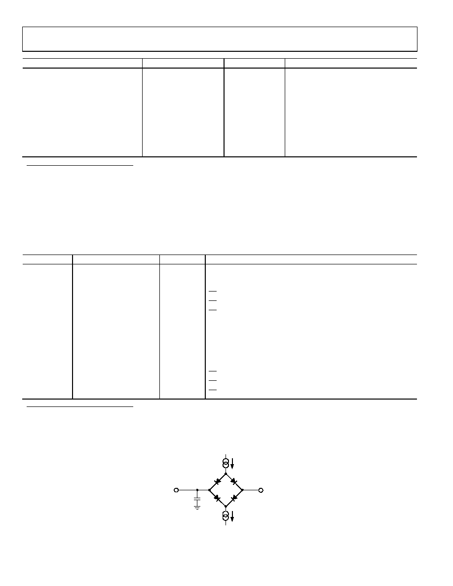
3 Measured with the load circuit in Figure 2 and defined as the time required for the output to cross 0.4 V or 2.0 V.
4 t12 is derived from the measured time taken by the data outputs to change 0.5 V when loaded with the circuit in Figure 2. The measured number is then extrapolated
back to remove the effects of charging or discharging the 50 pF capacitor. This means that the time, t12, quoted in the timing characteristics is the true bus relinquish
time of the part and is independent of the bus loading.
02144-B
-002
200
A
1.6V
200
A
IOL
IOH
TO
OUTPUT
PIN
CL
50pF
Figure 2. Load Circuit for Digital Output Timing Specifications
相關(guān)PDF資料 |
PDF描述 |
|---|---|
| GEC40DRYH-S13 | CONN EDGECARD 80POS .100 EXTEND |
| EVAL-AD7607EDZ | EVAL BOARD FOR AD7607 |
| GSC12DRTS-S13 | CONN EDGECARD 24POS .100 EXTEND |
| GMC12DRTS-S13 | CONN EDGECARD 24POS .100 EXTEND |
| 0210490306 | CABLE JUMPER 1.25MM .102M 24POS |
相關(guān)代理商/技術(shù)參數(shù) |
參數(shù)描述 |
|---|---|
| EVAL-AD7851CB | 制造商:Analog Devices 功能描述:14-BIT 333 KSPS SERIAL A/D CONVERTER 制造商:Analog Devices 功能描述:EVALUATION CONTROL BOARD I.C. - Bulk |
| EVAL-AD7851CB4 | 制造商:AD 制造商全稱:Analog Devices 功能描述:14-Bit 333 kSPS Serial A/D Converter |
| EVAL-AD7853CB | 制造商:Analog Devices 功能描述:EVALUATION CONTROL BOARD - Bulk |
| EVAL-AD7854CB | 制造商:Analog Devices 功能描述:EVALUATION CONTROL BOARD - Bulk |
| EVAL-AD7856CB | 制造商:AD 制造商全稱:Analog Devices 功能描述:5 V Single Supply, 8-Channel 14-Bit 285 kSPS Sampling ADC |
發(fā)布緊急采購,3分鐘左右您將得到回復(fù)。