- 您現(xiàn)在的位置:買賣IC網(wǎng) > PDF目錄1913 > DS1875T+T&R (Maxim Integrated Products)IC SFP CTRLR/TRIPLEXER 38-TQFN PDF資料下載
參數(shù)資料
| 型號: | DS1875T+T&R |
| 廠商: | Maxim Integrated Products |
| 文件頁數(shù): | 9/92頁 |
| 文件大小: | 0K |
| 描述: | IC SFP CTRLR/TRIPLEXER 38-TQFN |
| 產(chǎn)品培訓(xùn)模塊: | Lead (SnPb) Finish for COTS Obsolescence Mitigation Program |
| 標準包裝: | 2,500 |
| 應(yīng)用: | 光纖 |
| 接口: | I²C |
| 電源電壓: | 2.85 V ~ 3.9 V |
| 封裝/外殼: | 38-WFQFN 裸露焊盤 |
| 供應(yīng)商設(shè)備封裝: | 38-TQFN(5x7) |
| 包裝: | 帶卷 (TR) |
| 安裝類型: | 表面貼裝 |
第1頁第2頁第3頁第4頁第5頁第6頁第7頁第8頁當前第9頁第10頁第11頁第12頁第13頁第14頁第15頁第16頁第17頁第18頁第19頁第20頁第21頁第22頁第23頁第24頁第25頁第26頁第27頁第28頁第29頁第30頁第31頁第32頁第33頁第34頁第35頁第36頁第37頁第38頁第39頁第40頁第41頁第42頁第43頁第44頁第45頁第46頁第47頁第48頁第49頁第50頁第51頁第52頁第53頁第54頁第55頁第56頁第57頁第58頁第59頁第60頁第61頁第62頁第63頁第64頁第65頁第66頁第67頁第68頁第69頁第70頁第71頁第72頁第73頁第74頁第75頁第76頁第77頁第78頁第79頁第80頁第81頁第82頁第83頁第84頁第85頁第86頁第87頁第88頁第89頁第90頁第91頁第92頁
DS1875
DC Operation
When using autodetect mode or closed-loop mode,
BEN should be equal to VCC or long burst. In open-loop
mode, BEN should be ground or any burst length.
Modulation Control
The MOD output is an 8-bit scaleable voltage output
that interfaces with the MAX3643’s VMSET input. An
external resistor to ground from the MAX3643’s
MODSET pin sets the maximum current that the voltage
at the VMSET input can produce for a given output
range. This resistor value should be chosen to produce
the maximum modulation current the laser type requires
over temperature. Then the MOD output’s scaling is
used to calibrate the full-scale (FS) modulation output
to a particular laser’s requirements. This allows the
application to take full advantage of the MOD output’s
resolution. The modulation LUT can be programmed in
2°C increments over the -40°C to +102°C range.
Ranging of the MOD DAC is possible by programming
a single byte in Table 02h, Register 8Bh.
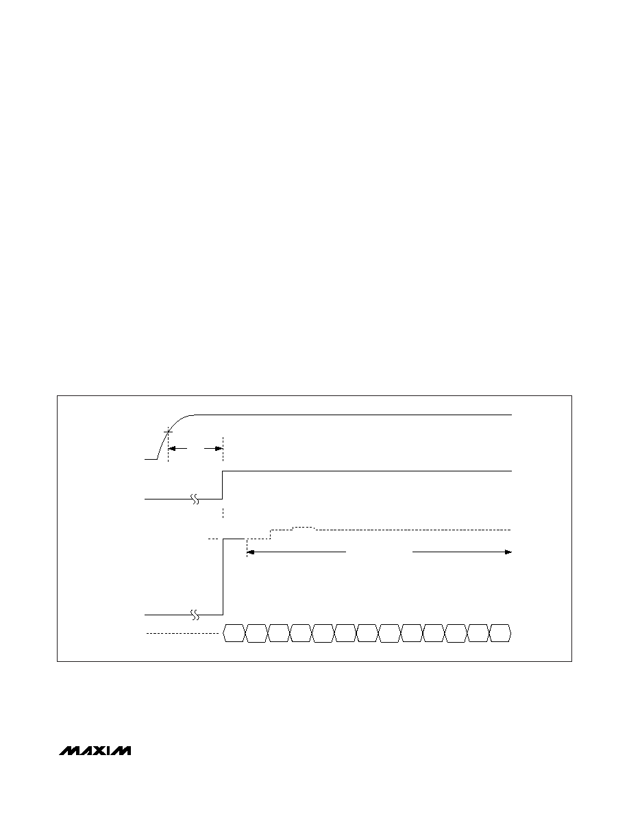
BIAS and MOD Output During Power-Up
On power-up the modulation and bias outputs remain off
until VCC is above VPOA, a temperature conversion has
been completed, and, if the VCC ADC alarm is enabled,
a VCC conversion above the customer-defined VCC low
alarm level must clear the VCC low alarm (tINIT). Once all
these conditions (tINIT) are satisfied, the MOD output is
enabled with the value determined by the temperature
conversion and the modulation LUT (Table 04h).
When the MOD output is enabled, the BIAS output is
turned on to a value equal to the temperature-indexed
value in the BIAS LUT (Table 08h). Next, the APC inte-
grator is enabled, and single LSB steps are taken to
tightly control the average power.
If a fault is detected and TX-D is toggled to re-enable
the outputs, the DS1875 powers up following a similar
sequence to an initial power-up. The only difference is
that the DS1875 already determined the present tem-
perature, so the tINIT time is not required for the
DS1875 to recall the APC and MOD set points from
EEPROM.
12
3
4
56
7
89
10
11
12
13
tINIT
VPOA
VMOD
IBIAS
VCC
BIAS
SAMPLE
APC INTEGRATOR ON
BIAS LUT
VALUE
Figure 1. Power-Up Timing (BEN is a Long Burst)
PON Triplexer and SFP Controller
______________________________________________________________________________________
17
相關(guān)PDF資料 |
PDF描述 |
|---|---|
| DS1876T+T&R | IC CTRLR SFP DUAL LDD 28TQFN |
| DS1877T+T&R | IC CTLR/MON SFP 1-2CH 28TQFN |
| DS1878T+T&R | IC CTLR SFP W/DGTL LDD RX 28TQFN |
| DS1881Z-050+T&R | IC DGTL POT NV 2CH 45K 16-SOIC |
| DS1882Z-050+T&R | IC POT DIGIT DL LOG 50K 16SOIC |
相關(guān)代理商/技術(shù)參數(shù) |
參數(shù)描述 |
|---|---|
| DS1876 | 制造商:MAXIM 制造商全稱:Maxim Integrated Products 功能描述:SFP Controller with Dual LDD Interface |
| DS1876T+ | 功能描述:ADC / DAC多通道 SFP+ Controller w/ Dual LDD Interface RoHS:否 制造商:Texas Instruments 轉(zhuǎn)換速率: 分辨率:8 bit 接口類型:SPI 電壓參考: 電源電壓-最大:3.6 V 電源電壓-最小:2 V 最大工作溫度:+ 85 C 安裝風(fēng)格:SMD/SMT 封裝 / 箱體:VQFN-40 |
| DS1876T+T&R | 制造商:Maxim Integrated Products 功能描述:SFP CTRLR W/DUAL LDD INTERFACE TQFN - Tape and Reel 制造商:Maxim Integrated Products 功能描述:IC CTRLR SFP DUAL LDD 28TQFN |
| DS1876T+T&R | 功能描述:ADC / DAC多通道 SFP+ Controller w/ Dual LDD Interface RoHS:否 制造商:Texas Instruments 轉(zhuǎn)換速率: 分辨率:8 bit 接口類型:SPI 電壓參考: 電源電壓-最大:3.6 V 電源電壓-最小:2 V 最大工作溫度:+ 85 C 安裝風(fēng)格:SMD/SMT 封裝 / 箱體:VQFN-40 |
| DS1876T+TR | 制造商:MAXIM 制造商全稱:Maxim Integrated Products 功能描述:SFP Controller with Dual LDD Interface |
發(fā)布緊急采購,3分鐘左右您將得到回復(fù)。