- 您現(xiàn)在的位置:買賣IC網(wǎng) > PDF目錄357735 > CY7C1041D-10ZSXC (CYPRESS SEMICONDUCTOR CORP) 256K X 16 STANDARD SRAM, 10 ns, PDSO44 PDF資料下載
參數(shù)資料
| 型號: | CY7C1041D-10ZSXC |
| 廠商: | CYPRESS SEMICONDUCTOR CORP |
| 元件分類: | SRAM |
| 英文描述: | 256K X 16 STANDARD SRAM, 10 ns, PDSO44 |
| 封裝: | LEAD FREE, TSOP2-44 |
| 文件頁數(shù): | 4/9頁 |
| 文件大小: | 206K |
| 代理商: | CY7C1041D-10ZSXC |
CY7C1041D
PRELIMINARY
Document #: 38-05472 Rev. *B
Page 4 of 9
Write Cycle
[8, 9]
t
WC
t
SCE
t
AW
t
HA
t
SA
t
PWE
t
SD
t
HD
t
LZWE
t
HZWE
t
BW
Write Cycle Time
CE LOW to Write End
Address Set-Up to Write End
Address Hold from Write End
Address Set-Up to Write Start
WE Pulse Width
Data Set-Up to Write End
Data Hold from Write End
WE HIGH to Low Z
[8]
WE LOW to High Z
[7, 8]
Byte Enable to End of Write
10
7
7
0
0
7
6
0
3
12
10
10
0
0
10
7
0
3
15
12
12
0
0
12
8
0
3
ns
ns
ns
ns
ns
ns
ns
ns
ns
ns
ns
6
6
7
7
10
12
Switching Characteristics
[5]
Over the Operating Range(continued)
7C1041D-10
Min.
7C1041D-12
Min.
7C1041D-15
Min.
Parameter
Description
Max.
Max.
Max.
Unit
Data Retention Characteristics
Over the Operating Range
Parameter
Description
Conditions
[11]
Min.
Max.
Unit
V
DR
V
CC
for Data Retention
2.0
V
I
CCDR
t
CDR[3]
t
R[10]
Data Retention Current
V
CC
= V
DR
= 2.0V,
CE > V
CC
– 0.3V,
V
IN
> V
CC
– 0.3V or V
IN
< 0.3V
10
mA
Chip Deselect to Data Retention Time
0
ns
Operation Recovery Time
t
RC
ns
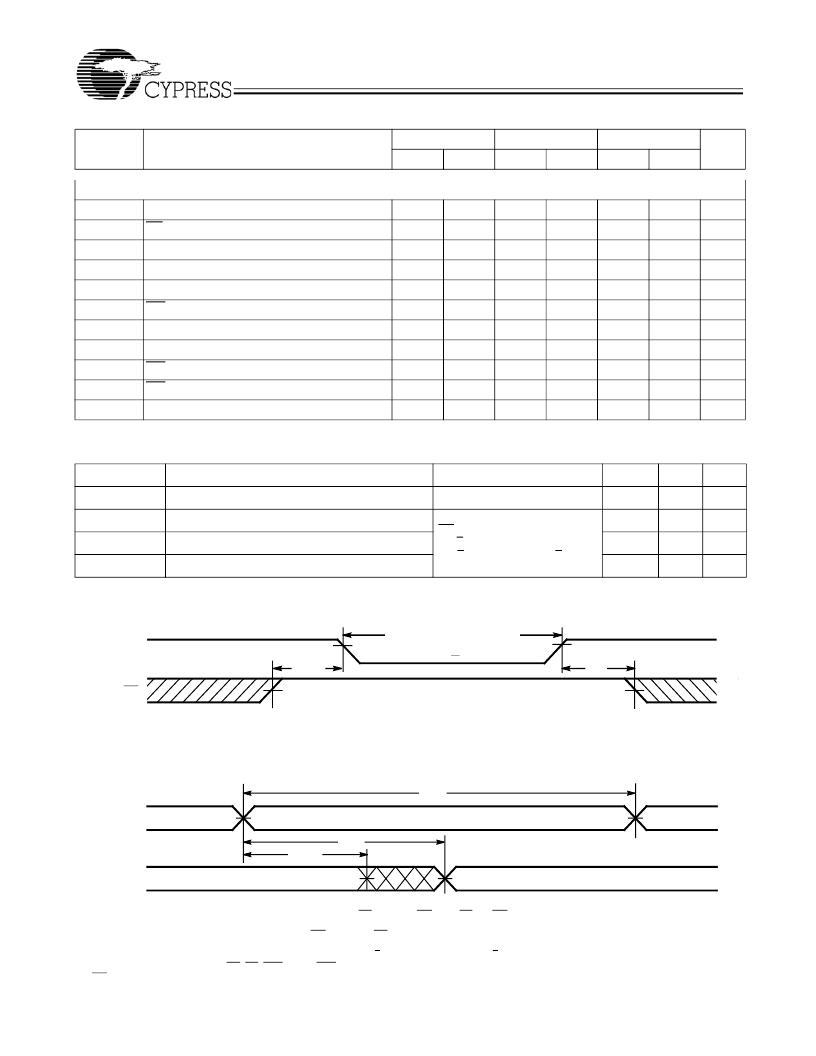
Data Retention Waveform
4.5V
4.5V
t
CDR
V
DR
> 2V
DATA RETENTION MODE
t
R
CE
V
CC
Switching Waveforms
Read Cycle No. 1
[12, 13]
PREVIOUS DATA VALID
DATA VALID
t
RC
t
AA
t
OHA
ADDRESS
DATA OUT
Notes:
8. The internal Write time of the memory is defined by the overlap of CE LOW, and WE LOW. CE and WE must be LOW to initiate a Write, and the transition of either
of these signals can terminate the Write. The input data set-up and hold timing should be referenced to the leading edge of the signal that terminates the Write.
9. The minimum Write cycle time for Write Cycle No. 3 (WE controlled, OE LOW) is the sum of t
HZWE
and t
SD
.
10.Full device operation requires linear V
CC
ramp from V
DR
to V
CC(min.)
> 50
μ
s or stable at V
CC(min.)
> 50
μ
s
11. No input may exceed V
+ 0.5V
12.Device is continuously selected. OE, CE, BHE, and/or BHE = V
IL
.
13.WE is HIGH for read cycle.
相關(guān)PDF資料 |
PDF描述 |
|---|---|
| CY7C166A-15PC | 16K X 4 STANDARD SRAM, 15 ns, PDIP24 |
| CY7C172A-25VCT | 4K X 4 STANDARD SRAM, 25 ns, PDSO24 |
| CY7C197-25LC | 256K X 1 STANDARD SRAM, 25 ns, CQCC28 |
| CY7C381-0JC | FPGA, 96 CLBS, 1000 GATES, PQCC44 |
| CY7C381-0JI | FPGA, 96 CLBS, 1000 GATES, PQCC44 |
相關(guān)代理商/技術(shù)參數(shù) |
參數(shù)描述 |
|---|---|
| CY7C1041D10ZSXI | 制造商:Cypress Semiconductor 功能描述: |
| CY7C1041D-10ZSXI | 功能描述:靜態(tài)隨機(jī)存取存儲器 4M FAST ASYNC HI SPD IND RoHS:否 制造商:Cypress Semiconductor 存儲容量:16 Mbit 組織:1 M x 16 訪問時(shí)間:55 ns 電源電壓-最大:3.6 V 電源電壓-最小:2.2 V 最大工作電流:22 uA 最大工作溫度:+ 85 C 最小工作溫度:- 40 C 安裝風(fēng)格:SMD/SMT 封裝 / 箱體:TSOP-48 封裝:Tray |
| CY7C1041D-10ZSXIT | 功能描述:靜態(tài)隨機(jī)存取存儲器 4M FAST ASYNC HI SPD IND RoHS:否 制造商:Cypress Semiconductor 存儲容量:16 Mbit 組織:1 M x 16 訪問時(shí)間:55 ns 電源電壓-最大:3.6 V 電源電壓-最小:2.2 V 最大工作電流:22 uA 最大工作溫度:+ 85 C 最小工作溫度:- 40 C 安裝風(fēng)格:SMD/SMT 封裝 / 箱體:TSOP-48 封裝:Tray |
| CY7C1041D-2XWI | 制造商:Cypress Semiconductor 功能描述: |
| CY7C1041DV33-10BVI | 功能描述:靜態(tài)隨機(jī)存取存儲器 4M FAST ASYNC HI SPD IND RoHS:否 制造商:Cypress Semiconductor 存儲容量:16 Mbit 組織:1 M x 16 訪問時(shí)間:55 ns 電源電壓-最大:3.6 V 電源電壓-最小:2.2 V 最大工作電流:22 uA 最大工作溫度:+ 85 C 最小工作溫度:- 40 C 安裝風(fēng)格:SMD/SMT 封裝 / 箱體:TSOP-48 封裝:Tray |
發(fā)布緊急采購,3分鐘左右您將得到回復(fù)。