- 您現(xiàn)在的位置:買賣IC網(wǎng) > PDF目錄384268 > CY2077ZI-XXX MISCELLANEOUS CLOCK GENERATOR|TSSOP|8PIN|PLASTIC PDF資料下載
參數(shù)資料
| 型號: | CY2077ZI-XXX |
| 英文描述: | MISCELLANEOUS CLOCK GENERATOR|TSSOP|8PIN|PLASTIC |
| 中文描述: | 雜項(xiàng)時(shí)鐘發(fā)生器| TSSOP封裝| 8引腳|塑料 |
| 文件頁數(shù): | 1/12頁 |
| 文件大小: | 305K |
| 代理商: | CY2077ZI-XXX |
High Accuracy EPROM Programmable
Single-PLL Clock Generator
CY2077
Cypress Semiconductor Corporation
3901 North First Street
San Jose
CA 95134
408-943-2600
January 24, 2001
either
Features
Benefits
High accuracy PLL with 12-bit multiplier and 10-bit
divider
EPROM-programmability
3.3V or 5V operation
Operating frequency
—390 kHz–133 MHz at 5V
—390 kHz–100 MHz at 3.3V
Reference input from either a 10-30 MHz fundamental
toned crystal or a 1-75 MHz external clock
Enables synthesis of highly accurate and stable output clock
frequencies with zero PPM
Enables quick turnaround of custom frequencies
Supports industry standard design platforms
Services most PC, networking, and consumer applications
Lowers cost of oscillator as PLL can be programmed to a high
frequency using either a low-frequency, low-cost crystal, or an
existing system clock
Duty cycle centered at 1.5V or V
DD
/2
Provides flexibility to service most TTL or CMOS applications
Provides flexibility in output configurations and testing
EPROM-selectable TTL or CMOS duty cycle levels
Sixteen selectable post-divide options, using either PLL
or reference oscillator/external clock
Programmable PWR_DWN or OE pin, with asynchro-
nous or synchronous modes
Enables low-power operation or output enable function and flex-
ibility for system applications, through selectable instantaneous
or synchronous change in outputs
Suitable for most PC, consumer, and networking applications
Low Jitter outputs typically
—80 ps at 3.3V/5V
Controlled rise and fall times and output slew rate
Available in both commercial and industrial temperature
Suitable to fit most applications
Factory-programmable device options
Has lower EMI than oscillators
Easy customization and fast turnaround.
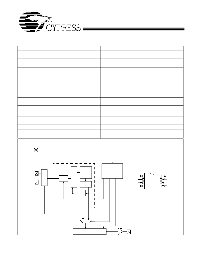
CY2077 Logic Block Diagram
XTALIN
or
external clock
PWR_DWN
XTALOUT
[1]
CONFIGURATION
EPROM
C
CLKOUT
/ 1, 2, 4, 8, 16, 32, 64, 128
O
or OE
MUX
HIGH
ACCURACY
PLL
1
2
3
4
5
8
7
6
VDD
XTALOUT
XTALIN
PD/OE
VSS
VSS
VSS
CLKOUT
8-Pin
Top View
Q
10 bits
P
12 bits
P
Charge
Pump
VCO
Note 1. When using an external clock source leave
XTALOUT floating
Pin Configuration
相關(guān)PDF資料 |
PDF描述 |
|---|---|
| CY2081ASC-XXX | MISCELLANEOUS CLOCK GENERATOR|SOP|8PIN|PLASTIC |
| CY2081ASL-XXX | MISCELLANEOUS CLOCK GENERATOR|SOP|8PIN|PLASTIC |
| CY2081SC | Interface IC |
| CY2081SL | Interface IC |
| CY2081WAF | MISCELLANEOUS CLOCK GENERATOR|DIE |
相關(guān)代理商/技術(shù)參數(shù) |
參數(shù)描述 |
|---|---|
| CY2077ZI-XXXT | 制造商:CYPRESS 制造商全稱:Cypress Semiconductor 功能描述:High-accuracy EPROM Programmable Single-PLL Clock Generator |
| CY2077ZXC-XXX | 制造商:CYPRESS 制造商全稱:Cypress Semiconductor 功能描述:High-accuracy EPROM Programmable Single-PLL Clock Generator |
| CY2077ZXC-XXXT | 制造商:CYPRESS 制造商全稱:Cypress Semiconductor 功能描述:High-accuracy EPROM Programmable Single-PLL Clock Generator |
| CY2077ZZ | 制造商:Cypress Semiconductor 功能描述: |
| CY2078-000 | 制造商:TE Connectivity 功能描述:44AM1121-20-9/96-2L-C2275 - Bulk |
發(fā)布緊急采購,3分鐘左右您將得到回復(fù)。