- 您現(xiàn)在的位置:買(mǎi)賣(mài)IC網(wǎng) > PDF目錄375308 > AM49LV6408MT10IT (SPANSION LLC) Stacked Multi-chip Package (MCP) 64 Mbit (4 M x 16 bit) Flash Memory and 8 Mbit (512K x 16-Bit) PDF資料下載
參數(shù)資料
| 型號(hào): | AM49LV6408MT10IT |
| 廠商: | SPANSION LLC |
| 元件分類(lèi): | 存儲(chǔ)器 |
| 英文描述: | Stacked Multi-chip Package (MCP) 64 Mbit (4 M x 16 bit) Flash Memory and 8 Mbit (512K x 16-Bit) |
| 中文描述: | SPECIALTY MEMORY CIRCUIT, PBGA69 |
| 封裝: | 10 X 8 MM, 1.20 MM HEIGHT, FBGA-69 |
| 文件頁(yè)數(shù): | 24/63頁(yè) |
| 文件大小: | 540K |
| 代理商: | AM49LV6408MT10IT |
第1頁(yè)第2頁(yè)第3頁(yè)第4頁(yè)第5頁(yè)第6頁(yè)第7頁(yè)第8頁(yè)第9頁(yè)第10頁(yè)第11頁(yè)第12頁(yè)第13頁(yè)第14頁(yè)第15頁(yè)第16頁(yè)第17頁(yè)第18頁(yè)第19頁(yè)第20頁(yè)第21頁(yè)第22頁(yè)第23頁(yè)當(dāng)前第24頁(yè)第25頁(yè)第26頁(yè)第27頁(yè)第28頁(yè)第29頁(yè)第30頁(yè)第31頁(yè)第32頁(yè)第33頁(yè)第34頁(yè)第35頁(yè)第36頁(yè)第37頁(yè)第38頁(yè)第39頁(yè)第40頁(yè)第41頁(yè)第42頁(yè)第43頁(yè)第44頁(yè)第45頁(yè)第46頁(yè)第47頁(yè)第48頁(yè)第49頁(yè)第50頁(yè)第51頁(yè)第52頁(yè)第53頁(yè)第54頁(yè)第55頁(yè)第56頁(yè)第57頁(yè)第58頁(yè)第59頁(yè)第60頁(yè)第61頁(yè)第62頁(yè)第63頁(yè)
22
Am49LV6408M
November 5, 2003
A D V A N C E I N F O R M A T I O N
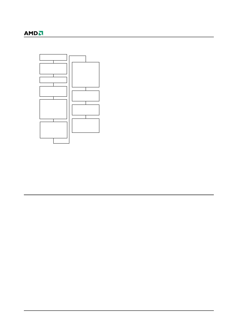
Figure 3.
SecSi Sector Protect Verify
Hardware Data Protection
The command sequence requirement of unlock cycles
for programming or erasing provides data protection
against inadvertent writes (refer to Tables
11
and
12
for command definitions). In addition, the following
hardware data protection measures prevent accidental
erasure or programming, which might otherwise be
caused by spurious system level signals during V
CC
power-up and power-down transitions, or from system
noise.
Low V
CC
Write Inhibit
When V
CC
is less than V
LKO
, the device does not ac-
cept any write cycles. This protects data during V
CC
power-up and power-down. The command register
and all internal program/erase circuits are disabled,
and the device resets to the read mode. Subsequent
writes are ignored until V
CC
is greater than V
LKO
. The
system must provide the proper signals to the control
pins to prevent unintentional writes when V
CC
is
greater than V
LKO
.
Write Pulse “Glitch” Protection
Noise pulses of less than 5 ns (typical) on OE#, CE#
or WE# do not initiate a write cycle.
Logical Inhibit
Write cycles are inhibited by holding any one of OE# =
V
IL
, CE# = V
IH
or WE# = V
IH
. To initiate a write cycle,
CE# and WE# must be a logical zero while OE# is a
logical one.
Power-Up Write Inhibit
If WE# = CE# = V
IL
and OE# = V
IH
during power up,
the device does not accept commands on the rising
edge of WE#. The internal state machine is automati-
cally reset to the read mode on power-up.
COMMON FLASH MEMORY INTERFACE (CFI)
The Common Flash Interface (CFI) specification out-
lines device and host system software interrogation
handshake, which allows specific vendor-specified
software algorithms to be used for entire families of
devices. Software support can then be device-inde-
pendent, JEDEC ID-independent, and forward- and
backward-compatible for the specified flash device
families. Flash vendors can standardize their existing
interfaces for long-term compatibility.
This device enters the CFI Query mode when the sys-
tem writes the CFI Query command, 98h, to address
55h, any time the device is ready to read array data.
The system can read CFI information at the addresses
given in Tables
7
–
10
. To terminate reading CFI data,
the system must write the reset command.
The system can also write the CFI query command
when the device is in the autoselect mode. The device
enters the CFI query mode, and the system can read
CFI data at the addresses given in Tables
7
–
10
. The
system must write the reset command to return the
device to reading array data.
For further information, please refer to the CFI Specifi-
cation and CFI Publication 100, available via the
World Wide Web at http://www.amd.com/flash/cfi. Al-
ternatively, contact an AMD representative for copies
of these documents.
Write 60h to
any address
Write 40h to SecSi
Sector address
with A6 = 0,
A1 = 1, A0 = 0
START
RESET# =
V
IH
or V
ID
Wait 1
μ
s
Read from SecSi
Sector address
with A6 = 0,
A1 = 1, A0 = 0
If data = 00h,
SecSi Sector is
unprotected.
If data = 01h,
SecSi Sector is
protected.
Remove V
or V
ID
from RESET#
Write reset
command
SecSi Sector
Protect Verify
complete
相關(guān)PDF資料 |
PDF描述 |
|---|---|
| AM49LV6408MT11IT | Stacked Multi-chip Package (MCP) 64 Mbit (4 M x 16 bit) Flash Memory and 8 Mbit (512K x 16-Bit) |
| AM49LV6408MT15IT | Stacked Multi-chip Package (MCP) 64 Mbit (4 M x 16 bit) Flash Memory and 8 Mbit (512K x 16-Bit) |
| AM49PDL127BH66IT | 128 Megabit (8 M x 16-Bit) CMOS 3.0 Volt-only, Simultaneous Operation Flash Memory and 32 Mbit (2 M x 16-Bit) CMOS |
| AM49PDL127BH85IS | 128 Megabit (8 M x 16-Bit) CMOS 3.0 Volt-only, Simultaneous Operation Flash Memory and 32 Mbit (2 M x 16-Bit) CMOS |
| AM49PDL127BH85IT | 128 Megabit (8 M x 16-Bit) CMOS 3.0 Volt-only, Simultaneous Operation Flash Memory and 32 Mbit (2 M x 16-Bit) CMOS |
相關(guān)代理商/技術(shù)參數(shù) |
參數(shù)描述 |
|---|---|
| AM49LV6408MT11I | 制造商:SPANSION 制造商全稱(chēng):SPANSION 功能描述:Stacked Multi-chip Package (MCP) 64 Mbit (4 M x 16 bit) Flash Memory and 8 Mbit (512K x 16-Bit) pseudo Static RAM |
| AM49LV6408MT11IT | 制造商:SPANSION 制造商全稱(chēng):SPANSION 功能描述:Stacked Multi-chip Package (MCP) 64 Mbit (4 M x 16 bit) Flash Memory and 8 Mbit (512K x 16-Bit) |
| AM49LV6408MT15I | 制造商:SPANSION 制造商全稱(chēng):SPANSION 功能描述:Stacked Multi-chip Package (MCP) 64 Mbit (4 M x 16 bit) Flash Memory and 8 Mbit (512K x 16-Bit) pseudo Static RAM |
| AM49LV6408MT15IT | 制造商:SPANSION 制造商全稱(chēng):SPANSION 功能描述:Stacked Multi-chip Package (MCP) 64 Mbit (4 M x 16 bit) Flash Memory and 8 Mbit (512K x 16-Bit) |
| AM49PDL127AH | 制造商:SPANSION 制造商全稱(chēng):SPANSION 功能描述:128 Megabit (8 M x 16-Bit) CMOS 3.0 Volt-only, Simultaneous Operation Flash Memory and 16 Mbit (1 M x 16-Bit) CMOS Pseudo Static RAM |
發(fā)布緊急采購(gòu),3分鐘左右您將得到回復(fù)。