- 您現(xiàn)在的位置:買賣IC網(wǎng) > PDF目錄375306 > AM42BDS640AGTD8IS (SPANSION LLC) Circular Connector; No. of Contacts:13; Series:MS27468; Body Material:Aluminum; Connecting Termination:Crimp; Connector Shell Size:11; Circular Contact Gender:Socket; Circular Shell Style:Jam Nut Receptacle; Insert Arrangement:11-35 RoHS Compliant: No PDF資料下載
參數(shù)資料
| 型號(hào): | AM42BDS640AGTD8IS |
| 廠商: | SPANSION LLC |
| 元件分類: | 存儲(chǔ)器 |
| 英文描述: | Circular Connector; No. of Contacts:13; Series:MS27468; Body Material:Aluminum; Connecting Termination:Crimp; Connector Shell Size:11; Circular Contact Gender:Socket; Circular Shell Style:Jam Nut Receptacle; Insert Arrangement:11-35 RoHS Compliant: No |
| 中文描述: | SPECIALTY MEMORY CIRCUIT, PBGA93 |
| 封裝: | 8 X 11.60 MM, FBGA-93 |
| 文件頁數(shù): | 34/72頁 |
| 文件大小: | 1060K |
| 代理商: | AM42BDS640AGTD8IS |
第1頁第2頁第3頁第4頁第5頁第6頁第7頁第8頁第9頁第10頁第11頁第12頁第13頁第14頁第15頁第16頁第17頁第18頁第19頁第20頁第21頁第22頁第23頁第24頁第25頁第26頁第27頁第28頁第29頁第30頁第31頁第32頁第33頁當(dāng)前第34頁第35頁第36頁第37頁第38頁第39頁第40頁第41頁第42頁第43頁第44頁第45頁第46頁第47頁第48頁第49頁第50頁第51頁第52頁第53頁第54頁第55頁第56頁第57頁第58頁第59頁第60頁第61頁第62頁第63頁第64頁第65頁第66頁第67頁第68頁第69頁第70頁第71頁第72頁
November 1, 2002
Am42BDS640AG
33
P R E L I M I N A R Y
II is valid after the rising edge of the final WE# pulse in
the command sequence.
DQ2 toggles when the system reads at addresses
within those sectors that have been selected for era-
sure. But DQ2 cannot distinguish whether the sector is
actively erasing or is erase-suspended. DQ6, by com-
parison, indicates whether the device is actively
erasing, or is in Erase Suspend, but cannot distinguish
which sectors are selected for erasure. Thus, both
status bits are required for sector and mode informa-
tion. Refer to
Table 15
to compare outputs for DQ2 and
DQ6.
See the following for additional information:
Figure 5,
“Toggle Bit Algorithm,” on page 32, See “DQ6: Toggle
Bit I” on page 32., Figure 28, “Toggle Bit Timings
(During Embedded Algorithm),” on page 57
, and
Table 15, “DQ6 and DQ2 Indications,” on page 33
.
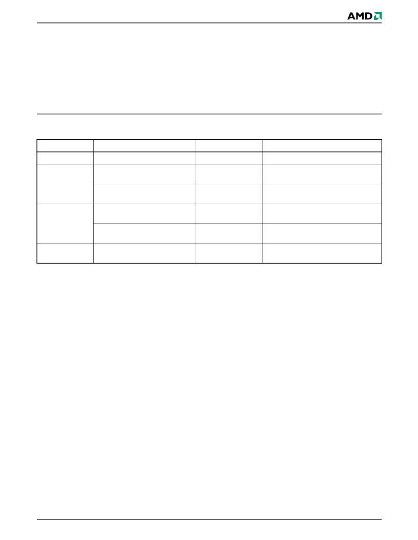
Table 15.
DQ6 and DQ2 Indications
Reading Toggle Bits DQ6/DQ2
Refer to Figure 4 for the following discussion. When-
ever the system initially begins reading toggle bit
status, it must read DQ7–DQ0 at least twice in a row to
determine whether a toggle bit is toggling. Typically, the
system would note and store the value of the toggle bit
after the first read. After the second read, the system
would compare the new value of the toggle bit with the
first. If the toggle bit is not toggling, the device has com-
pleted the program or erase operation. The system can
read array data on DQ7–DQ0 on the following read
cycle.
However, if after the initial two read cycles, the system
determines that the toggle bit is still toggling, the
system also should note whether the value of DQ5 is
high (see the section on DQ5). If it is, the system
should then determine again whether the toggle bit is
toggling, since the toggle bit may have stopped tog-
gling just as DQ5 went high. If the toggle bit is no longer
toggling, the device has successfully completed the
program or erase operation. If it is still toggling, the
device did not completed the operation successfully,
and the system must write the reset command to return
to reading array data.
The remaining scenario is that the system initially
determines that the toggle bit is toggling and DQ5 has
not gone high. The system may continue to monitor the
toggle bit and DQ5 through successive read cycles,
determining the status as described in the previous
paragraph. Alternatively, it may choose to perform
other system tasks. In this case, the system must start
at the beginning of the algorithm when it returns to
determine the status of the operation (top of Figure 4).
DQ5: Exceeded Timing Limits
DQ5 indicates whether the program or erase time has
exceeded a specified internal pulse count limit. Under
these conditions DQ5 produces a “1,” indicating that
the program or erase cycle was not successfully com-
pleted.
The device may output a “1” on DQ5 if the system tries
to program a “1” to a location that was previously pro-
grammed to “0.” Only an erase operation can change a
“0” back to a “1.” Under this condition, the device halts
the operation, and when the timing limit has been
exceeded, DQ5 produces a “1.”
Under both these conditions, the system must write the
reset command to return to the read mode (or to the
erase-suspend-read mode if a bank was previously in
the erase-suspend-program mode).
If device is
and the system reads
then DQ6
and DQ2
programming,
at any address,
toggles,
does not toggle.
actively erasing,
at an address within a sector
selected for erasure,
toggles,
also toggles.
at an address within sectors
not
selected for erasure,
toggles,
does not toggle.
erase suspended,
at an address within a sector
selected for erasure,
does not toggle,
toggles.
at an address within sectors
not
selected for erasure,
returns array data,
returns array data. The system can read
from any sector not selected for erasure.
programming in
erase suspend
at any address,
toggles,
is not applicable.
相關(guān)PDF資料 |
PDF描述 |
|---|---|
| AM42BDS640AGTD8IT | Circular Connector; No. of Contacts:13; Series:MS27468; Body Material:Aluminum; Connecting Termination:Crimp; Connector Shell Size:11; Circular Contact Gender:Socket; Circular Shell Style:Jam Nut Receptacle; Insert Arrangement:11-35 RoHS Compliant: No |
| AM42BDS640AGBD8IS | RES 93.1K-OHM 0.1% 0.125W 50PPM THIN-FILM SMD-1206 TR-7-PL ROHS |
| AM42BDS640AGBD8IT | Stacked Multi-Chip Package (MCP) Flash Memory and SRAM |
| AM42BDS640AGTD9IS | LJT 13C 13#22D SKT WALL RECP |
| AM42BDS640AGTD9IT | Stacked Multi-Chip Package (MCP) Flash Memory and SRAM |
相關(guān)代理商/技術(shù)參數(shù) |
參數(shù)描述 |
|---|---|
| AM42BDS640AGTD8IT | 制造商:AMD 制造商全稱:Advanced Micro Devices 功能描述:64 Megabit (4 M x 16-Bit) CMOS 1.8 Volt-only, Simultaneous Operation, Burst Mode Flash Memory and 16 Mbit (1 M x 16-Bit) Static RAM |
| AM42BDS640AGTD9IS | 制造商:AMD 制造商全稱:Advanced Micro Devices 功能描述:64 Megabit (4 M x 16-Bit) CMOS 1.8 Volt-only, Simultaneous Operation, Burst Mode Flash Memory and 16 Mbit (1 M x 16-Bit) Static RAM |
| AM42BDS640AGTD9IT | 制造商:AMD 制造商全稱:Advanced Micro Devices 功能描述:64 Megabit (4 M x 16-Bit) CMOS 1.8 Volt-only, Simultaneous Operation, Burst Mode Flash Memory and 16 Mbit (1 M x 16-Bit) Static RAM |
| AM42DL1612DB30IS | 制造商:AMD 制造商全稱:Advanced Micro Devices 功能描述:Am29DL16xD 16 Megabit (2 M x 8-Bit/1 M x 16-Bit) CMOS 3.0 Volt-only, Simultaneous Operation Flash Memory and 2 Mbit (128 K x 16-Bit) Static RAM |
| AM42DL1612DB30IT | 制造商:AMD 制造商全稱:Advanced Micro Devices 功能描述:Am29DL16xD 16 Megabit (2 M x 8-Bit/1 M x 16-Bit) CMOS 3.0 Volt-only, Simultaneous Operation Flash Memory and 2 Mbit (128 K x 16-Bit) Static RAM |
發(fā)布緊急采購,3分鐘左右您將得到回復(fù)。