- 您現(xiàn)在的位置:買(mǎi)賣(mài)IC網(wǎng) > PDF目錄375292 > AM29DL320GB70WMIN (SPANSION LLC) DIODE SCHOTTKY SINGLE 10V 200mW 0.37V-vf 30mA-IFM 1mA-IF 1uA-IR SOT-323 3K/REEL PDF資料下載
參數(shù)資料
| 型號(hào): | AM29DL320GB70WMIN |
| 廠商: | SPANSION LLC |
| 元件分類(lèi): | DRAM |
| 英文描述: | DIODE SCHOTTKY SINGLE 10V 200mW 0.37V-vf 30mA-IFM 1mA-IF 1uA-IR SOT-323 3K/REEL |
| 中文描述: | 2M X 16 FLASH 3V PROM, 70 ns, PBGA48 |
| 封裝: | 6 X 12 MM, 0.80 MM PITCH, FBGA-48 |
| 文件頁(yè)數(shù): | 30/58頁(yè) |
| 文件大小: | 1239K |
| 代理商: | AM29DL320GB70WMIN |
第1頁(yè)第2頁(yè)第3頁(yè)第4頁(yè)第5頁(yè)第6頁(yè)第7頁(yè)第8頁(yè)第9頁(yè)第10頁(yè)第11頁(yè)第12頁(yè)第13頁(yè)第14頁(yè)第15頁(yè)第16頁(yè)第17頁(yè)第18頁(yè)第19頁(yè)第20頁(yè)第21頁(yè)第22頁(yè)第23頁(yè)第24頁(yè)第25頁(yè)第26頁(yè)第27頁(yè)第28頁(yè)第29頁(yè)當(dāng)前第30頁(yè)第31頁(yè)第32頁(yè)第33頁(yè)第34頁(yè)第35頁(yè)第36頁(yè)第37頁(yè)第38頁(yè)第39頁(yè)第40頁(yè)第41頁(yè)第42頁(yè)第43頁(yè)第44頁(yè)第45頁(yè)第46頁(yè)第47頁(yè)第48頁(yè)第49頁(yè)第50頁(yè)第51頁(yè)第52頁(yè)第53頁(yè)第54頁(yè)第55頁(yè)第56頁(yè)第57頁(yè)第58頁(yè)
28
Am29DL320G
September 27, 2004
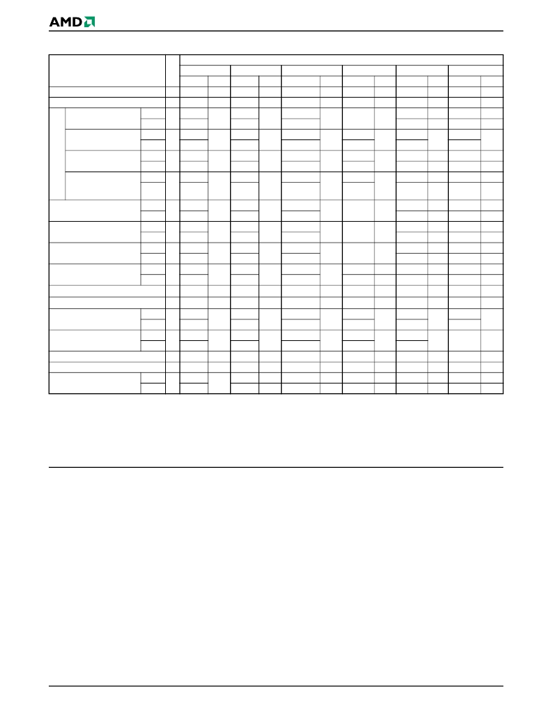
Table 13.
Command Definitions
Legend:
X = Don’t care
RA = Address of the memory location to be read.
RD = Data read from location RA during read operation.
PA = Address of the memory location to be programmed. Addresses
latch on the falling edge of the WE# or CE# pulse, whichever happens
later.
PD = Data to be programmed at location PA. Data latches on the rising
edge of WE# or CE# pulse, whichever happens first.
SA = Address of the sector to be verified (in autoselect mode) or
erased. Address bits A20–A12 uniquely select any sector.
BA = Address of the bank that is being switched to autoselect mode, is
in bypass mode, or is being erased.
Notes:
1.
2.
3.
See
Table 1
for description of bus operations.
All values are in hexadecimal.
Except for the read cycle and the fourth cycle of the autoselect
command sequence, all bus cycles are write cycles.
Data bits DQ15–DQ8 are don’t care in command sequences,
except for RD and PD.
Unless otherwise noted, address bits A20–A11 are don’t cares.
No unlock or command cycles required when bank is reading
array data.
The Reset command is required to return to the read mode (or to
the erase-suspend-read mode if previously in Erase Suspend)
when a bank is in the autoselect mode, or if DQ5 goes high (while
the bank is providing status information).
The fourth cycle of the autoselect command sequence is a read
cycle. The system must provide the bank address to obtain the
manufacturer ID, device ID, or SecSi Sector factory protect
information. Data bits DQ15–DQ8 are don’t care. See the
Autoselect Command Sequence
section for more information.
4.
5.
6.
7.
8.
9.
The device ID must be read across three cycles. The device ID is
00h for bottom boot devices, and 01h for top boot devices.
10. The data is 82h for factory locked and 02h for not factory locked.
11. The data is 00h for an unprotected sector/sector block and 01h for
a protected sector/sector block.
12. The Unlock Bypass command is required prior to the Unlock
Bypass Program command.
13. The Unlock Bypass Reset command is required to return to the
read mode when the bank is in the unlock bypass mode.
14. The system may read and program in non-erasing sectors, or
enter the autoselect mode, when in the Erase Suspend mode.
The Erase Suspend command is valid only during a sector erase
operation, and requires the bank address.
15. The Erase Resume command is valid only during the Erase
Suspend mode, and requires the bank address.
16. Command is valid when device is ready to read array data or when
device is in autoselect mode.
Command
Sequence
(Note 1)
C
Bus Cycles (Notes 2–5)
Third
Addr
Data
First
Second
Addr
Fourth
Addr
Fifth
Sixth
Addr
RA
XXX
555
AAA
555
AAA
555
AAA
555
Data
RD
F0
Data
Data
Addr
Data
Addr
Data
Read (Note 6)
Reset (Note 7)
1
1
A
Manufacturer ID
Word
Byte
Word
Byte
Word
Byte
Word
4
AA
2AA
555
2AA
555
2AA
555
2AA
55
(BA)555
(BA)AAA
(BA)555
(BA)AAA
(BA)555
(BA)AAA
(BA)555
90
(BA)X00
01
Device ID (Note 9)
4
AA
55
90
(BA)X01
(BA)X02
(BA)X03
(BA)X06
(SA)X02
7E
(BA)X0E
(BA)X1C
0A
(BA)X0F
(BA)X1E
00/
01
SecSi
Sector Factory
Protect (Note 10)
Sector/Sector Block
Protect Verify
(Note 11)
4
AA
55
90
82/02
4
AA
55
90
00/01
Byte
AAA
555
(BA)AAA
(SA)X04
Enter SecSi Sector Region
Word
Byte
Word
Byte
Word
Byte
Word
Byte
3
555
AAA
555
AAA
555
AAA
555
AAA
XXX
AA
2AA
555
2AA
555
2AA
555
2AA
555
PA
55
555
AAA
555
AAA
555
AAA
555
AAA
88
Exit SecSi Sector Region
4
AA
55
90
XXX
00
Program
4
AA
55
A0
PA
PD
Unlock Bypass
3
AA
55
20
Unlock Bypass Program (Note 12)
2
2
A0
PD
Unlock Bypass Reset (Note 13)
BA
555
AAA
555
AAA
BA
BA
55
AA
90
XXX
2AA
555
2AA
555
00
Chip Erase
Word
Byte
Word
Byte
6
AA
55
555
AAA
555
AAA
80
555
AAA
555
AAA
AA
2AA
555
2AA
555
55
555
AAA
10
Sector Erase
6
AA
55
80
AA
55
SA
30
Erase Suspend (Note 14)
Erase Resume (Note 15)
1
1
B0
30
CFI Query (Note 16)
Word
Byte
1
98
相關(guān)PDF資料 |
PDF描述 |
|---|---|
| AM29DL320GT70WMFN | For new designs involving TSOP packages, S29JL032H supercedes Am29DL320G and is the factory-recommended migration path. |
| AM29DL320GB70WMFN | For new designs involving TSOP packages, S29JL032H supercedes Am29DL320G and is the factory-recommended migration path. |
| AM29DL322GT120WMIN | 32 Megabit (4 M x 8-Bit/2 M x 16-Bit) CMOS 3.0 Volt-only, Simultaneous Operation Flash Memory |
| AM29DL322GB120EF | 32 Megabit (4 M x 8-Bit/2 M x 16-Bit) CMOS 3.0 Volt-only, Simultaneous Operation Flash Memory |
| AM29DL322GB120EI | 32 Megabit (4 M x 8-Bit/2 M x 16-Bit) CMOS 3.0 Volt-only, Simultaneous Operation Flash Memory |
相關(guān)代理商/技術(shù)參數(shù) |
參數(shù)描述 |
|---|---|
| AM29DL322DB7REIT | 制造商:AMD 功能描述:New |
| AM29DL322DB-90WDIT | 制造商:Spansion 功能描述:FLASH PARALLEL 3V/3.3V 32MBIT 4MX8/2MX16 90NS 63FBGA - Tape and Reel |
| AM29DL322DT-90EI-T | 制造商:Advanced Micro Devices 功能描述: |
| AM29DL322GB-90EI | 制造商:Advanced Micro Devices 功能描述:2M X 16 FLASH 3V PROM, 90 ns, 48 Pin Plastic SMT |
| AM29DL322GT-90EI | 制造商:Advanced Micro Devices 功能描述:Flash Mem Parallel 3.3V 32M-Bit 4M x 8/2M x 16 90ns 48-Pin TSOP |
發(fā)布緊急采購(gòu),3分鐘左右您將得到回復(fù)。