- 您現(xiàn)在的位置:買賣IC網(wǎng) > PDF目錄375292 > AM29DL320GB70WMIN (SPANSION LLC) DIODE SCHOTTKY SINGLE 10V 200mW 0.37V-vf 30mA-IFM 1mA-IF 1uA-IR SOT-323 3K/REEL PDF資料下載
參數(shù)資料
| 型號(hào): | AM29DL320GB70WMIN |
| 廠商: | SPANSION LLC |
| 元件分類: | DRAM |
| 英文描述: | DIODE SCHOTTKY SINGLE 10V 200mW 0.37V-vf 30mA-IFM 1mA-IF 1uA-IR SOT-323 3K/REEL |
| 中文描述: | 2M X 16 FLASH 3V PROM, 70 ns, PBGA48 |
| 封裝: | 6 X 12 MM, 0.80 MM PITCH, FBGA-48 |
| 文件頁(yè)數(shù): | 28/58頁(yè) |
| 文件大?。?/td> | 1239K |
| 代理商: | AM29DL320GB70WMIN |
第1頁(yè)第2頁(yè)第3頁(yè)第4頁(yè)第5頁(yè)第6頁(yè)第7頁(yè)第8頁(yè)第9頁(yè)第10頁(yè)第11頁(yè)第12頁(yè)第13頁(yè)第14頁(yè)第15頁(yè)第16頁(yè)第17頁(yè)第18頁(yè)第19頁(yè)第20頁(yè)第21頁(yè)第22頁(yè)第23頁(yè)第24頁(yè)第25頁(yè)第26頁(yè)第27頁(yè)當(dāng)前第28頁(yè)第29頁(yè)第30頁(yè)第31頁(yè)第32頁(yè)第33頁(yè)第34頁(yè)第35頁(yè)第36頁(yè)第37頁(yè)第38頁(yè)第39頁(yè)第40頁(yè)第41頁(yè)第42頁(yè)第43頁(yè)第44頁(yè)第45頁(yè)第46頁(yè)第47頁(yè)第48頁(yè)第49頁(yè)第50頁(yè)第51頁(yè)第52頁(yè)第53頁(yè)第54頁(yè)第55頁(yè)第56頁(yè)第57頁(yè)第58頁(yè)
26
Am29DL320G
September 27, 2004
V
HH
on the WP#/ACC pin, the device automatically en-
ters the Unlock Bypass mode. The system may then
write the two-cycle Unlock Bypass program command
sequence. The device uses the higher voltage on the
WP#/ACC pin to accelerate the operation. Note that
the WP#/ACC pin must not be at V
HH
any operation
other than accelerated programming, or device dam-
age may result. In addition, the WP#/ACC pin must not
be left floating or unconnected; inconsistent behavior
of the device may result.
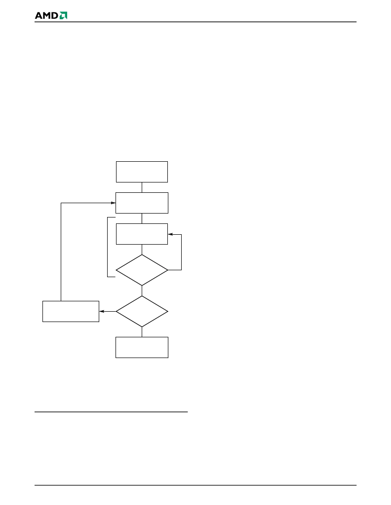
Figure 4
illustrates the algorithm for the program oper-
ation. Refer to the Erase and Program Operations
table in the AC Characteristics section for parameters,
and
Figure 18
for timing diagrams.
Figure 4.
Program Operation
Chip Erase Command Sequence
Chip erase is a six bus cycle operation. The chip erase
command sequence is initiated by writing two unlock
cycles, followed by a set-up command. Two additional
unlock write cycles are then followed by the chip erase
command, which in turn invokes the Embedded Erase
algorithm. The device does
not
require the system to
preprogram prior to erase. The Embedded Erase algo-
rithm automatically preprograms and verifies the entire
memory for an all zero data pattern prior to electrical
erase. The system is not required to provide any con-
trols or timings during these operations.
Table 13
shows the address and data requirements for the chip
erase command sequence.
When the Embedded Erase algorithm is complete,
that bank returns to the read mode and addresses are
no longer latched. The system can determine the sta-
tus of the erase operation by using DQ7, DQ6, DQ2,
or RY/BY#. Refer to the Write Operation Status sec-
tion for information on these status bits.
Any commands written during the chip erase operation
are ignored. However, note that a
hardware reset
im-
mediately terminates the erase operation. If that oc-
curs, the chip erase command sequence should be
reinitiated once that bank has returned to reading
array data, to ensure data integrity.
Figure 5
illustrates the algorithm for the erase opera-
tion. Refer to the Erase and Program Operations ta-
bles in the AC Characteristics section for parameters,
and
Figure 20
section for timing diagrams.
Sector Erase Command Sequence
Sector erase is a six bus cycle operation. The sector
erase command sequence is initiated by writing two
unlock cycles, followed by a set-up command. Two ad-
ditional unlock cycles are written, and are then fol-
lowed by the address of the sector to be erased, and
the sector erase command.
Table 13
shows the ad-
dress and data requirements for the sector erase com-
mand sequence.
The device does
not
require the system to preprogram
prior to erase. The Embedded Erase algorithm auto-
matically programs and verifies the entire memory for
an all zero data pattern prior to electrical erase. The
system is not required to provide any controls or tim-
ings during these operations.
After the command sequence is written, a sector erase
time-out of 50 μs occurs. During the time-out period,
additional sector addresses and sector erase com-
mands (for sectors within the same bank) may be writ-
ten. Loading the sector erase buffer may be done in
any sequence, and the number of sectors may be from
one sector to all sectors. The time between these ad-
ditional cycles must be less than 50 μs, otherwise era-
sure may begin. Any sector erase address and
command following the exceeded time-out may or may
not be accepted. It is recommended that processor in-
terrupts be disabled during this time to ensure all com-
mands are accepted. The interrupts can be re-enabled
after the last Sector Erase command is written.
Any
command other than Sector Erase or Erase Sus-
START
Write Program
Command Sequence
Data Poll
from System
Verify Data
No
Yes
Last Address
No
Yes
Programming
Completed
Increment Address
Embedded
Program
algorithm
in progress
Note:
See
Table 13
for program command sequence.
相關(guān)PDF資料 |
PDF描述 |
|---|---|
| AM29DL320GT70WMFN | For new designs involving TSOP packages, S29JL032H supercedes Am29DL320G and is the factory-recommended migration path. |
| AM29DL320GB70WMFN | For new designs involving TSOP packages, S29JL032H supercedes Am29DL320G and is the factory-recommended migration path. |
| AM29DL322GT120WMIN | 32 Megabit (4 M x 8-Bit/2 M x 16-Bit) CMOS 3.0 Volt-only, Simultaneous Operation Flash Memory |
| AM29DL322GB120EF | 32 Megabit (4 M x 8-Bit/2 M x 16-Bit) CMOS 3.0 Volt-only, Simultaneous Operation Flash Memory |
| AM29DL322GB120EI | 32 Megabit (4 M x 8-Bit/2 M x 16-Bit) CMOS 3.0 Volt-only, Simultaneous Operation Flash Memory |
相關(guān)代理商/技術(shù)參數(shù) |
參數(shù)描述 |
|---|---|
| AM29DL322DB7REIT | 制造商:AMD 功能描述:New |
| AM29DL322DB-90WDIT | 制造商:Spansion 功能描述:FLASH PARALLEL 3V/3.3V 32MBIT 4MX8/2MX16 90NS 63FBGA - Tape and Reel |
| AM29DL322DT-90EI-T | 制造商:Advanced Micro Devices 功能描述: |
| AM29DL322GB-90EI | 制造商:Advanced Micro Devices 功能描述:2M X 16 FLASH 3V PROM, 90 ns, 48 Pin Plastic SMT |
| AM29DL322GT-90EI | 制造商:Advanced Micro Devices 功能描述:Flash Mem Parallel 3.3V 32M-Bit 4M x 8/2M x 16 90ns 48-Pin TSOP |
發(fā)布緊急采購(gòu),3分鐘左右您將得到回復(fù)。