- 您現(xiàn)在的位置:買賣IC網(wǎng) > PDF目錄374037 > ADSP-2195MBST-140X (ANALOG DEVICES INC) DSP Microcomputer PDF資料下載
參數(shù)資料
| 型號: | ADSP-2195MBST-140X |
| 廠商: | ANALOG DEVICES INC |
| 元件分類: | 數(shù)字信號處理 |
| 英文描述: | DSP Microcomputer |
| 中文描述: | 16-BIT, 160 MHz, OTHER DSP, PQFP144 |
| 封裝: | METRIC, PLASTIC, LQFP-144 |
| 文件頁數(shù): | 55/68頁 |
| 文件大小: | 951K |
| 代理商: | ADSP-2195MBST-140X |
第1頁第2頁第3頁第4頁第5頁第6頁第7頁第8頁第9頁第10頁第11頁第12頁第13頁第14頁第15頁第16頁第17頁第18頁第19頁第20頁第21頁第22頁第23頁第24頁第25頁第26頁第27頁第28頁第29頁第30頁第31頁第32頁第33頁第34頁第35頁第36頁第37頁第38頁第39頁第40頁第41頁第42頁第43頁第44頁第45頁第46頁第47頁第48頁第49頁第50頁第51頁第52頁第53頁第54頁當前第55頁第56頁第57頁第58頁第59頁第60頁第61頁第62頁第63頁第64頁第65頁第66頁第67頁第68頁
This information applies to a product under development. Its characteristics and specifications are subject to change with-
out notice. Analog Devices assumes no obligation regarding future manufacturing unless otherwise agreed to in writing.
55
REV. PrA
For current information contact Analog Devices at 800/262-5643
ADSP-2195
September 2001
Example System Hold
Time Calculation
To determine the data output
hold time in a particular
system, first calculate t
DECAY
using the equation given in
Figure 31
. Choose –V to be
the difference between the
ADSP-2195’s output voltage
and the input threshold for
the device requiring the hold
time. A typical –V will be
0.4 V. C
L
is the total bus
capacitance (per data line),
and I
L
is the total leakage or
three-state current (per data
line). The hold time will be
t
DECAY
plus the minimum
disable time (i.e., t
DATRWH
for
the write cycle).
Capacitive Loading
Output delays and holds are
based on standard capacitive
loads: 50 pF on all pins (see
Figure 37
). The delay and
hold specifications given
should be derated by a factor
of 1.5 ns/50 pF for loads
other than the nominal value
of 50 pF.
Figure 35
and
Figure 36
show how output
rise time varies with capaci-
tance. These figures also
show graphically how output
delays and holds vary with
load capacitance. (Note that
this graph or derating does
not apply to output disable
delays; see
Output Disable
Time on page 54
.) The
graphs in these figures may
not be linear outside the
ranges shown.
Environmental Conditions
The thermal characteristics
in which the DSP is operating
influence performance.
Thermal Characteristics
The ADSP-2195 comes in a
144-lead LQFP or 144-lead
Ball Grid Array (mini-BGA)
package. The ADSP-2195 is
specified for an ambient tem-
perature (T
AMB
) as calculated
using the formula in
Figure 38
. To ensure that the
T
AMB
data sheet specification
is not exceeded, a heatsink
and/or an air flow source may
be used. A heatsink should be
attached to the ground plane
(as close as possible to the
thermal pathways) with a
thermal adhesive.
Where:
T
AMB
= Ambient tempera-
ture (measured near top
surface of package)
PD = Power dissipation in
W (this value depends
upon the specific applica-
tion; a method for
calculating PD is shown
under Power Dissipation).
θ
CA
= Value from
Table 25
.
θ
JB
= TBD°C/W
There are some important
things to note about these
T
AMB
calculations and the
values in
Table 25
:
This represents thermal
resistance at total power of
TBDW.
For the LQFP package:
θ
JC
= 0.96°C/W
For the mini-BGA
package:
θ
JC
= 8.4°C/W
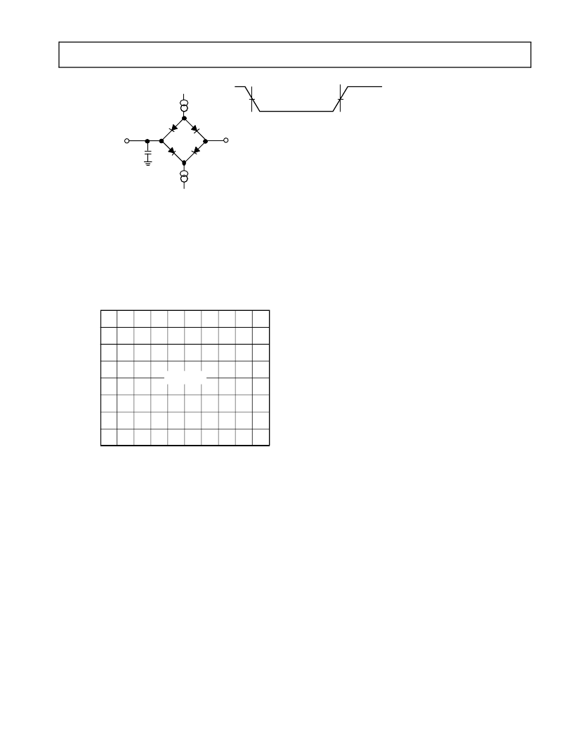
Figure 33. Equivalent
Device Loading
for AC
Measurements
(Includes All
Fixtures)
:.)(
)';
FiguVoltaReferenLevefAC
MEnable/Disable)
(Except
Output
.)(
.)(
Figure 35. Typical Output Rise Time (10%–90%,
V
DDEXT
=Max) vs. Load Capacitance
*;
.'
.'
'
'
''
'
'
'
'
''
'
'
'
'
.'
.'
.'
.'
'.'
.'
*
<
'
(
(
相關(guān)PDF資料 |
PDF描述 |
|---|---|
| ADSP-2195 | LM2991 Negative Low Dropout Adjustable Regulator; Package: CERDIP; No of Pins: 16; Qty per Container: 25; Container: Rail |
| ADSP-2195MBCA-140X | LM2991 Negative Low Dropout Adjustable Regulator; Package: CERDIP; No of Pins: 16; Container: Rail |
| ADSP-2195MKST-160X | LM2991 Negative Low Dropout Adjustable Regulator; Package: TO-263; No of Pins: 5; Qty per Container: 45; Container: Rail |
| ADSP-2196 | DSP Microcomputer |
| ADSP-2196MBCA-140X | DSP Microcomputer |
相關(guān)代理商/技術(shù)參數(shù) |
參數(shù)描述 |
|---|---|
| ADSP-2195MKCA-160 | 制造商:Analog Devices 功能描述:DSP Fixed-Point 24-Bit 160MHz 160MIPS 144-Pin CSP-BGA 制造商:Rochester Electronics LLC 功能描述:16-BIT,160 MIPS, 2.5V, 80KBYTES RAM - Bulk |
| ADSP-2195MKST-160 | 制造商:Analog Devices 功能描述:DSP Fixed-Point 24-Bit 160MHz 160MIPS 144-Pin LQFP 制造商:Analog Devices 功能描述:IC MICROCOMPUTER 16-BIT |
| adsp-2196mbca-140 | 制造商:Analog Devices 功能描述: |
| adsp-2196mbst-140 | 制造商:Analog Devices 功能描述:DSP Fixed-Point 16-Bit 140MHz 140MIPS 144-Pin LQFP 制造商:Rochester Electronics LLC 功能描述: |
| ADSP-2196MBST-140Z | 制造商:Analog Devices 功能描述:DSP Fixed-Point 16-Bit 140MHz 140MIPS 144-Pin LQFP |
發(fā)布緊急采購,3分鐘左右您將得到回復。