- 您現(xiàn)在的位置:買賣IC網(wǎng) > PDF目錄374035 > ADSP-2171KST-133 (ANALOG DEVICES INC) DSP Microcomputer PDF資料下載
參數(shù)資料
| 型號: | ADSP-2171KST-133 |
| 廠商: | ANALOG DEVICES INC |
| 元件分類: | 數(shù)字信號處理 |
| 英文描述: | DSP Microcomputer |
| 中文描述: | 24-BIT, 16.67 MHz, OTHER DSP, PQFP128 |
| 封裝: | PLASTIC, TQFP-128 |
| 文件頁數(shù): | 7/52頁 |
| 文件大小: | 664K |
| 代理商: | ADSP-2171KST-133 |
第1頁第2頁第3頁第4頁第5頁第6頁當(dāng)前第7頁第8頁第9頁第10頁第11頁第12頁第13頁第14頁第15頁第16頁第17頁第18頁第19頁第20頁第21頁第22頁第23頁第24頁第25頁第26頁第27頁第28頁第29頁第30頁第31頁第32頁第33頁第34頁第35頁第36頁第37頁第38頁第39頁第40頁第41頁第42頁第43頁第44頁第45頁第46頁第47頁第48頁第49頁第50頁第51頁第52頁
ADSP-2171/ADSP-2172/ADSP-2173
REV. A
–7–
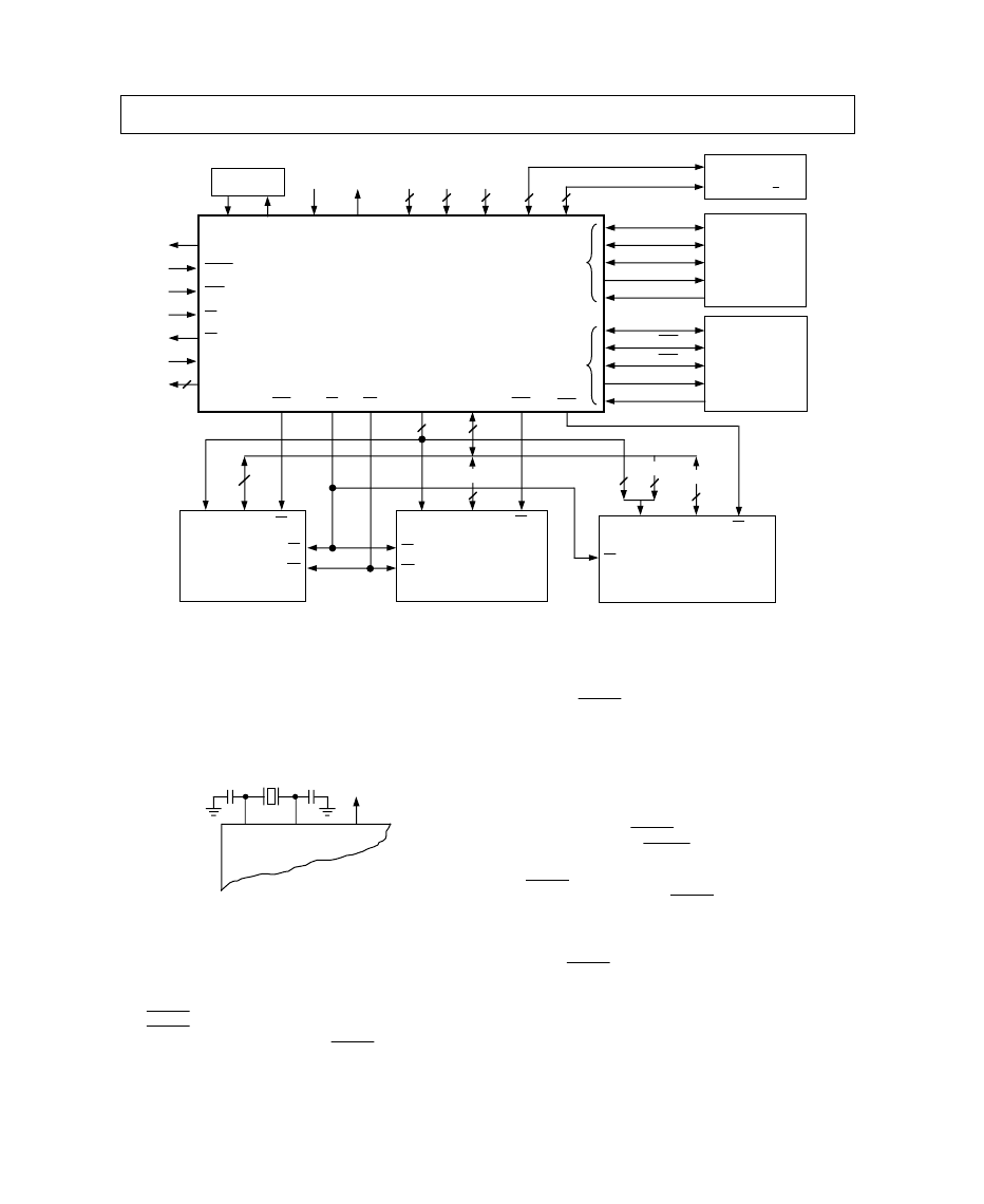
Figure 3. ADSP-217x Basic System Configuration
Because the ADSP-217x includes an on-chip oscillator circuit,
an external crystal may be used. T he crystal should be con-
nected across the CLK IN and X T AL pins, with two capacitors
connected as shown in Figure 4. A parallel-resonant, fundamen-
tal frequency, microprocessor-grade crystal should be used.
CLKIN
CLKOUT
XTAL
ADSP-217x
Figure 4. External Crystal Connections
A clock output (CLK OUT ) signal is generated by the processor
at the processor’s cycle rate. T his can be enabled and disabled
by the CLK ODIS bit in the SPORT 0 Autobuffer Control Reg-
ister, DM[0x3FF3].
Reset
T he
RESET
signal initiates a master reset of the ADSP-217x.
T he
RESET
signal must be asserted during the power-up se-
quence to assure proper initialization.
RESET
during initial
power-up must be held long enough to allow the internal clock
SCLK
RFS
TFS
DT
DR
ADSP-217x
CLKIN
CLKOUT
V
DD
SERIAL
PORT 0
GND
SERIAL
PORT 1
DATA
ADDRESS
PMS
DMS
BMS
RD
WR
14
24
16
8
24
SERIAL DEVICE
14
2
XTAL
MMAP
BG
BR
IRQ2
RESET
SCLK
RFS or
IRQ0
TFS or
IRQ1
DT or FO
DR or FI
A
D
CS
DATA MEMORY
&
PERIPHERALS
(OPTIONAL)
A
D
CS
OE
WE
PROGRAM
MEMORY
(OPTIONAL)
NOTE:
THE TWO MSBs OF THE DATA BUS ARE USED AS THE MSBs OF THE BOOT EPROM ADDRESS.
THIS IS ONLY REQUIRED FOR THE 27C256 AND 27C512.
A
D
BOOT MEMORY
e.g., EPROM
27C64
27C128
27C256
27C512
SERIAL DEVICE
(OPTIONAL)
(OPTIONAL)
D
15-8
HOST
MODE
FL2-0
4
6
9
7
16
HOST
PROCESSOR
(OPTIONAL)
3
HIP CONTROL
HIP
HIP DATA/ADDR
PWDACK
PWD
CLOCK OR
CRYSTAL
D
23-22
D
23-8
OE
WE
OE
CS
to stabilize. If
RESET
is activated any time after power-up, the
clock continues to run and does not require stabilization time.
T he power-up sequence is defined as the total time required for
the crystal oscillator circuit to stabilize after a valid V
DD
is ap-
plied to the processor, and for the internal phase-locked loop
(PLL) to lock onto the specific crystal frequency. A minimum of
2000 CLK IN cycles ensures that the PLL has locked but does
not include the crystal oscillator start-up time. During this
power-up sequence the
RESET
signal should be held low. On
any subsequent resets, the
RESET
signal must meet the mini-
mum pulse width specification, t
RSP
.
T he
RESET
input contains some hysteresis; however, if you use
an RC circuit to generate your
RESET
signal, the use of an ex-
ternal Schmidt trigger is recommended.
T he master reset sets all internal stack pointers to the empty
stack condition, masks all interrupts and clears the MST AT reg-
ister. When
RESET
is released, if there is no pending bus re-
quest and the chip is configured for booting (MMAP = 0), the
boot-loading sequence is performed. T hen the first instruction is
fetched from internal program memory location 0x0000.
相關(guān)PDF資料 |
PDF描述 |
|---|---|
| ADSP-2171BST-104 | DSP Microcomputer |
| ADSP-2171BST-133 | DSP Microcomputer |
| ADSP-2173BS-80 | DSP Microcomputer |
| ADSP-2171 | DSP Microcomputer(DSP 微計算機) |
| ADSP-2172 | DSP Microcomputer(DSP 微計算機) |
相關(guān)代理商/技術(shù)參數(shù) |
參數(shù)描述 |
|---|---|
| ADSP-2172 | 制造商:AD 制造商全稱:Analog Devices 功能描述:DSP Microcomputer |
| ADSP-2173 | 制造商:AD 制造商全稱:Analog Devices 功能描述:DSP Microcomputer |
| ADSP-2173BS-80 | 制造商:Rochester Electronics LLC 功能描述:- Bulk |
| ADSP-2173BST-80 | 制造商:Analog Devices 功能描述:DSP Fixed-Point 16-Bit 20MHz 20MIPS 128-Pin TQFP 制造商:Rochester Electronics LLC 功能描述:16BIT FXD PT PROC 3.3V - Bulk |
| ADSP-2176-760040 | 制造商:Analog Devices 功能描述: |
發(fā)布緊急采購,3分鐘左右您將得到回復(fù)。