- 您現(xiàn)在的位置:買賣IC網(wǎng) > PDF目錄375263 > ADS1271EVM (Texas Instruments, Inc.) modular EVM form factor PDF資料下載
參數(shù)資料
| 型號: | ADS1271EVM |
| 廠商: | Texas Instruments, Inc. |
| 英文描述: | modular EVM form factor |
| 中文描述: | 模塊化EVM的外形 |
| 文件頁數(shù): | 23/29頁 |
| 文件大小: | 381K |
| 代理商: | ADS1271EVM |
第1頁第2頁第3頁第4頁第5頁第6頁第7頁第8頁第9頁第10頁第11頁第12頁第13頁第14頁第15頁第16頁第17頁第18頁第19頁第20頁第21頁第22頁當(dāng)前第23頁第24頁第25頁第26頁第27頁第28頁第29頁
SBAS306A NOVEMBER 2004 REVISED DECEMBER 2004
www.ti.com
23
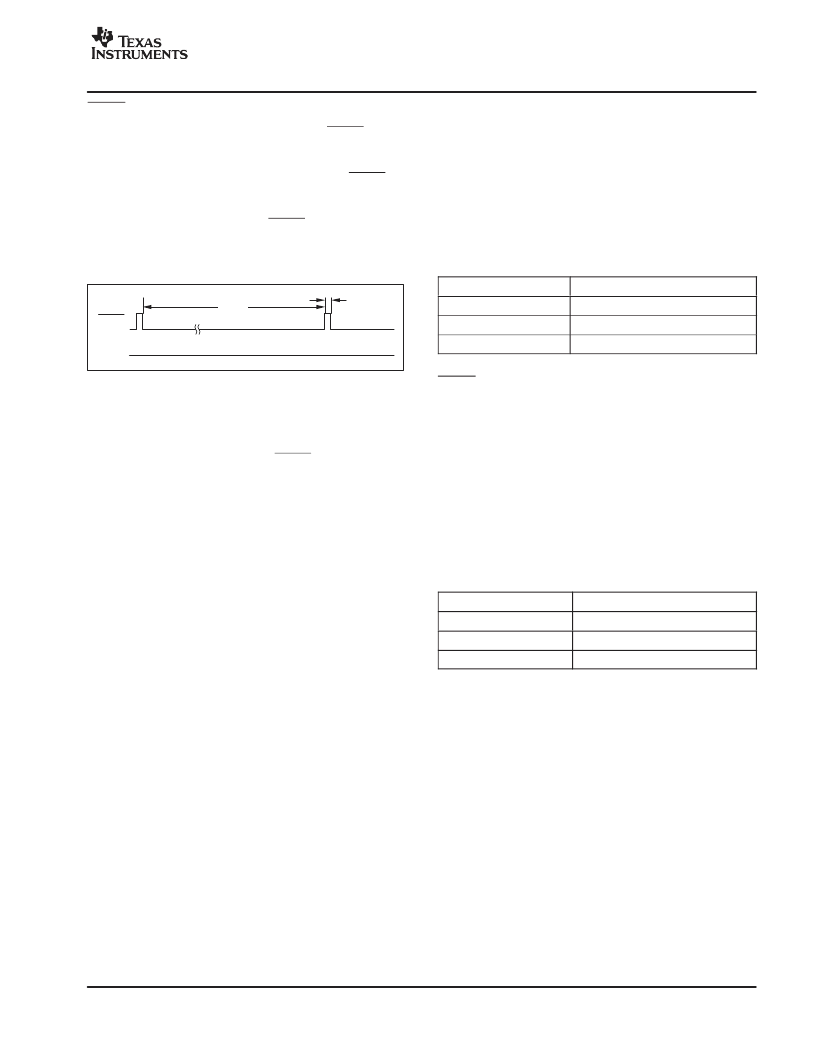
DRDY/FSYNC
In the SPI format, this pin functions as the DRDY output.
It goes low when data is ready for retrieval and then returns
high on the rising edge of the first subsequent SCLK. If
data is not retrieved (that is, SCLK is held low), DRDY will
pulse high just before the next conversion data is ready, as
shown in Figure 57. The new data is loaded within the
ADS1271 one CLK cycle before DRDY goes low. All data
must be shifted out before this time to avoid being
overwritten.
DRDY
SCLK
1/f
DATA
1/f
CLK
Figure 57. DRDY Timing with No Readback
DOUT
The conversion data is shifted out on DOUT. The MSB
data is valid on DOUT when DRDY goes low. The
subsequent bits are shifted out with each falling edge of
SCLK. If daisy-chaining, the data shifted in using DIN will
appear on DOUT after all 24 bits have been shifted out.
DIN
This input is used when multiple ADS1271s are to be
daisy-chained together. The DOUT pin of the first device
connects to the DIN pin of the next, etc. It can be used with
either the SPI or Frame-Sync formats. Data is shifted in on
the falling edge of SCLK. When using only one ADS1271,
tie DIN low. See the
Daisy-Chaining
section for more
information.
FRAME-SYNC SERIAL INTERFACE
Frame-Sync format is similar to the interface often used on
audio ADCs. It operates in
slave
fashion—the user must
supply framing signal FSYNC (similar to the
left/right clock
on stereo audio ADCs) and the serial clock SCLK (similar
to the
bit clock
on audio ADCs). The data is output MSB
first or
left-justified
. When using Frame-Sync format, the
CLK, FSYNC and SCLK inputs must be synchronized
together, as described in the following sub-sections.
SCLK (Frame-Sync Format)
The serial clock (SCLK) features a Schmitt-triggered input
and shifts out data on DOUT on the falling edge. It also
shifts in data on the falling edge on DIN when this pin is
being used for daisy-chaining. Even though SCLK has
hysteresis, it is recommended to keep SCLK as clean as
possible to prevent glitches from accidentally shifting the
data. When using Frame-Sync format, SCLK must run
continuously. If it is shut down, the data readback will be
corrupted. Frame-Sync format requires a specific
relationship between SCLK and FSYNC, determined by
the mode shown in Table 10.
Table 10. SCLK Period When Using Frame-Sync
Format
MODE
REQUIRED SCLK PERIOD
High-Speed
τ
FRAME/64
τ
FRAME/128
τ
FRAME/64
High-Resolution
Low-Power
DRDY/FSYNC
In Frame-Sync format, this pin is used as the FSYNC input.
The frame-sync input (FSYNC) sets the frame period. The
required FSYNC periods are shown in Table 11. For
High-Speed mode, the FSYNC period must be 256 CLK
periods. For both High-Resolution and Low-Power modes,
the FSYNC period can be either 512 or 256 CLK periods;
the ADS1271 will automatically detect which is being
used. If the FSYNC period is not the proper value, data
readback will be corrupted. It is recommended that
FSYNC be aligned with the falling edge of SCLK.
Table 11. FSYNC Period
MODE
REQUIRED FSYNC PERIOD
High-Speed
256 CLK Periods
High-Resolution
256 or 512 CLK periods
Low-Power
256 or 512 CLK periods
DOUT
The conversion data is shifted out on DOUT. The MSB
data becomes valid on DOUT on the SCLK rising edge
prior to FSYNC going high. The subsequent bits are
shifted out with each falling edge of SCLK. If
daisy-chaining, the data shifted in using DIN will appear on
DOUT after all 24 bits have been shifted out.
DIN
This input is used when multiple ADS1271s are to be
daisy-chained together. It can be used with either SPI or
Frame-Sync formats. Data is shifted in on the falling edge
of SCLK. When using only one ADS1271, tie DIN low.See
the
Daisy-Chaining
section for more information.
相關(guān)PDF資料 |
PDF描述 |
|---|---|
| ADS1601 | 16-BIT 1.25MSPS ANALOG TO DIGITAL CONVERTER |
| ADS1601IPFBR | 16-BIT 1.25MSPS ANALOG TO DIGITAL CONVERTER |
| ADS1601IPFBT | 16-BIT 1.25MSPS ANALOG TO DIGITAL CONVERTER |
| ADS1602 | 16-Bit, 2.5MSPS Analog-to-Digital Converter |
| ADS1602IPFBR | 16-Bit, 2.5MSPS Analog-to-Digital Converter |
相關(guān)代理商/技術(shù)參數(shù) |
參數(shù)描述 |
|---|---|
| ADS1271EVM-PDK | 功能描述:數(shù)據(jù)轉(zhuǎn)換 IC 開發(fā)工具 ADS1271 Eval Mod RoHS:否 制造商:Texas Instruments 產(chǎn)品:Demonstration Kits 類型:ADC 工具用于評估:ADS130E08 接口類型:SPI 工作電源電壓:- 6 V to + 6 V |
| ADS1271IBPW | 功能描述:模數(shù)轉(zhuǎn)換器 - ADC 24B 105kSPS Indus Delta-Sigma ADC RoHS:否 制造商:Texas Instruments 通道數(shù)量:2 結(jié)構(gòu):Sigma-Delta 轉(zhuǎn)換速率:125 SPs to 8 KSPs 分辨率:24 bit 輸入類型:Differential 信噪比:107 dB 接口類型:SPI 工作電源電壓:1.7 V to 3.6 V, 2.7 V to 5.25 V 最大工作溫度:+ 85 C 安裝風(fēng)格:SMD/SMT 封裝 / 箱體:VQFN-32 |
| ADS1271IBPW | 制造商:Texas Instruments 功能描述:24BIT ADC 105KSPS DELTA S 16TSSOP 制造商:Texas Instruments 功能描述:24BIT ADC, 105KSPS, DELTA S, 16TSSOP 制造商:Texas Instruments 功能描述:24BIT ADC, 105KSPS, DELTA S, 16TSSOP; Resolution (Bits):24bit; Sampling Rate:105kSPS; Supply Voltage Type:Single; Supply Voltage Min:4.75V; Supply Voltage Max:5.25V; Supply Current:17mA; Digital IC Case Style:TSSOP; No. of Pins:16; ;RoHS Compliant: Yes |
| ADS1271IBPWG4 | 功能描述:模數(shù)轉(zhuǎn)換器 - ADC 24B 105kSPS Indus Delta-Sigma ADC RoHS:否 制造商:Texas Instruments 通道數(shù)量:2 結(jié)構(gòu):Sigma-Delta 轉(zhuǎn)換速率:125 SPs to 8 KSPs 分辨率:24 bit 輸入類型:Differential 信噪比:107 dB 接口類型:SPI 工作電源電壓:1.7 V to 3.6 V, 2.7 V to 5.25 V 最大工作溫度:+ 85 C 安裝風(fēng)格:SMD/SMT 封裝 / 箱體:VQFN-32 |
| ADS1271IBPWR | 功能描述:模數(shù)轉(zhuǎn)換器 - ADC 24B 105kSPS Indus Delta-Sigma ADC RoHS:否 制造商:Texas Instruments 通道數(shù)量:2 結(jié)構(gòu):Sigma-Delta 轉(zhuǎn)換速率:125 SPs to 8 KSPs 分辨率:24 bit 輸入類型:Differential 信噪比:107 dB 接口類型:SPI 工作電源電壓:1.7 V to 3.6 V, 2.7 V to 5.25 V 最大工作溫度:+ 85 C 安裝風(fēng)格:SMD/SMT 封裝 / 箱體:VQFN-32 |
發(fā)布緊急采購,3分鐘左右您將得到回復(fù)。