- 您現(xiàn)在的位置:買賣IC網(wǎng) > PDF目錄375262 > ADP3401 (Analog Devices, Inc.) 2nd Level Over Voltage Protection for 2, 3, or 4 Cell LiIon & LiPoly Batteries (2nd Lev Protection) 8-TSSOP -25 to 85 PDF資料下載
參數(shù)資料
| 型號: | ADP3401 |
| 廠商: | Analog Devices, Inc. |
| 英文描述: | 2nd Level Over Voltage Protection for 2, 3, or 4 Cell LiIon & LiPoly Batteries (2nd Lev Protection) 8-TSSOP -25 to 85 |
| 中文描述: | 手機(jī)電源管理系統(tǒng) |
| 文件頁數(shù): | 5/12頁 |
| 文件大?。?/td> | 281K |
| 代理商: | ADP3401 |
ADP3401
–5–
REV. 0
ABSOLUTE MAXIMUM RATINGS
*
Voltage on Any Pin with Respect
to Any GND Pin . . . . . . . . . . . . . . . . . . . . . . –0.3 V, +10 V
Voltage on Any Pin May Not Exceed VBAT,
with the Following Exceptions: VRTC, VSIM,
CAP+, PWRONIN, I/O, CLK, RST
Storage Temperature Range . . . . . . . . . . . . –65
°
C to +150
°
C
Operating Temperature Range . . . . . . . . . . . –20
°
C to +85
°
C
Maximum Junction Temperature . . . . . . . . . . . . . . . . .125
°
C
θ
JA
, Thermal Impedance (TSSOP-28) . . 2-Layer Board 90
°
C/W
θ
JA
, Thermal Impedance (TSSOP-28) . . 4-Layer Board 60
°
C/W
Lead Temperature Range (Soldering, 60 sec) . . . . . . . . 300
°
C
*
This is a stress rating only, operation beyond these limits can cause the device to
be permanently damaged.
CAUTION
ESD (electrostatic discharge) sensitive device. Electrostatic charges as high as 4000 V readily
accumulate on the human body and test equipment and can discharge without detection.
Although the ADP3401 features proprietary ESD protection circuitry, permanent damage may
occur on devices subjected to high energy electrostatic discharges. Therefore, proper ESD
precautions are recommended to avoid performance degradation or loss of functionality.
WARNING!
ESD SENSITIVE DEVICE
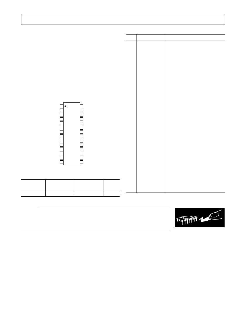
PIN CONFIGURATION
28
27
26
25
24
23
22
21
20
19
18
17
16
15
1
2
3
4
5
6
7
8
9
10
11
12
13
14
ADP3401
SIMGND
CLKIN
RESETIN
DATAIO
SIMBAT
CAP
2
VRTC
VBAT
VCC
PWRONKEY
ANALOGON
CHRON
ROWX
PWRONIN
I/O
RST
SIMPROG
SIMON
CLK
VSIM
CAP+
AGND
VCCA
REFOUT
RESET
RESCAP
DGND
VTCXO
PIN FUNCTION DESCRIPTIONS
Pin
Mnemonic
Function
1
2
3
4
5
VBAT
VCC
PWRONKEY
ANALOGON
PWRONIN
Battery Input Voltage
Digital Low Dropout Regulator
Power On/Off Key
VTCXO Enable
Power On/Off Signal from
Microprocessor
Microprocessor Keyboard Output
Charger On/Off Input
Real-Time Clock Supply/Coin
Cell Battery Charger
Negative Side of Boost Capacitor
Battery Input for the SIM
Charge Pump
Non-Level-Shifted Bidirectional
Data I/O
Non-Level-Shifted SIM Reset
Non-Level-Shifted Clock
Charge Pump Ground
Level-Shifted BidirectionalSIM
Data Input/Output
Level-Shifted SIM Reset
VSIM Programming:
Low = 3 V, High = 5 V
VSIM Enable
Level-Shifted SIM Clock
SIM Supply
Positive Side of Boost Capacitor
Reset Delay Timing Cap
Digital Ground
Crystal Oscillator Low Dropout
Regulator
Main Reset
Reference Output
Analog Low Dropout Regulator
Analog Ground
6
7
8
ROWX
CHRON
VRTC
9
10
CAP–
SIMBAT
11
DATAIO
12
13
14
15
RESETIN
CLKIN
SIMGND
I/O
16
17
RST
SIMPROG
18
19
20
21
22
23
24
SIMON
CLK
VSIM
CAP+
RESCAP
DGND
VTCXO
25
26
27
28
RESET
REFOUT
VCCA
AGND
ORDERING GUIDE
Temperature
Range
Package
Description
Package
Option
Model
ADP3401ARU –20
°
C to +85
°
C
28-Lead TSSOP
RU-28A
相關(guān)PDF資料 |
PDF描述 |
|---|---|
| ADP3401ARU | 2nd Level Over Voltage Protection for 2, 3, or 4 Cell LiIon & LiPoly Batteries (2nd Lev Protection) 8-TSSOP -25 to 85 |
| ADP3402 | Replaced by BQ29412 : Voltage Protection for 2-,3-or,4-Cell Lion Batteries (2nd Protection) 8-SM8 -20 to 85 |
| ADP3402ARU | Replaced by BQ29412 : Voltage Protection for 2-,3-or,4-Cell Lion Batteries (2nd Protection) 8-SM8 |
| ADP3418KRZ-REEL1 | Dual Bootstrapped 12 V MOSFET Driver with Output Disable |
| ADP3418KRZ1 | Dual Bootstrapped 12 V MOSFET Driver with Output Disable |
相關(guān)代理商/技術(shù)參數(shù) |
參數(shù)描述 |
|---|---|
| ADP3401ARU | 制造商:AD 制造商全稱:Analog Devices 功能描述:GSM Power Management System |
| ADP3401ARU-REEL | 制造商:Analog Devices 功能描述:GSM Power Management System Li-Ion/NiMH 2.765V 28-Pin TSSOP T/R |
| ADP3401ARU-REEL OPT | 制造商:Analog Devices 功能描述: |
| ADP3402 | 制造商:AD 制造商全稱:Analog Devices 功能描述:GSM Power Management System |
| ADP3402ARU | 制造商:AD 制造商全稱:Analog Devices 功能描述:GSM Power Management System |
發(fā)布緊急采購,3分鐘左右您將得到回復(fù)。