- 您現(xiàn)在的位置:買(mǎi)賣(mài)IC網(wǎng) > PDF目錄373979 > ADE7169ACPF16 (ANALOG DEVICES INC) Single-Phase Energy Measurement IC with 8052 MCU, RTC and LCD driver PDF資料下載
參數(shù)資料
| 型號(hào): | ADE7169ACPF16 |
| 廠商: | ANALOG DEVICES INC |
| 元件分類(lèi): | 模擬信號(hào)調(diào)理 |
| 英文描述: | Single-Phase Energy Measurement IC with 8052 MCU, RTC and LCD driver |
| 中文描述: | ANALOG CIRCUIT, QCC64 |
| 封裝: | 9 X 9MM, MO-220VMMD, LFCSP-64 |
| 文件頁(yè)數(shù): | 44/140頁(yè) |
| 文件大小: | 1359K |
| 代理商: | ADE7169ACPF16 |
第1頁(yè)第2頁(yè)第3頁(yè)第4頁(yè)第5頁(yè)第6頁(yè)第7頁(yè)第8頁(yè)第9頁(yè)第10頁(yè)第11頁(yè)第12頁(yè)第13頁(yè)第14頁(yè)第15頁(yè)第16頁(yè)第17頁(yè)第18頁(yè)第19頁(yè)第20頁(yè)第21頁(yè)第22頁(yè)第23頁(yè)第24頁(yè)第25頁(yè)第26頁(yè)第27頁(yè)第28頁(yè)第29頁(yè)第30頁(yè)第31頁(yè)第32頁(yè)第33頁(yè)第34頁(yè)第35頁(yè)第36頁(yè)第37頁(yè)第38頁(yè)第39頁(yè)第40頁(yè)第41頁(yè)第42頁(yè)第43頁(yè)當(dāng)前第44頁(yè)第45頁(yè)第46頁(yè)第47頁(yè)第48頁(yè)第49頁(yè)第50頁(yè)第51頁(yè)第52頁(yè)第53頁(yè)第54頁(yè)第55頁(yè)第56頁(yè)第57頁(yè)第58頁(yè)第59頁(yè)第60頁(yè)第61頁(yè)第62頁(yè)第63頁(yè)第64頁(yè)第65頁(yè)第66頁(yè)第67頁(yè)第68頁(yè)第69頁(yè)第70頁(yè)第71頁(yè)第72頁(yè)第73頁(yè)第74頁(yè)第75頁(yè)第76頁(yè)第77頁(yè)第78頁(yè)第79頁(yè)第80頁(yè)第81頁(yè)第82頁(yè)第83頁(yè)第84頁(yè)第85頁(yè)第86頁(yè)第87頁(yè)第88頁(yè)第89頁(yè)第90頁(yè)第91頁(yè)第92頁(yè)第93頁(yè)第94頁(yè)第95頁(yè)第96頁(yè)第97頁(yè)第98頁(yè)第99頁(yè)第100頁(yè)第101頁(yè)第102頁(yè)第103頁(yè)第104頁(yè)第105頁(yè)第106頁(yè)第107頁(yè)第108頁(yè)第109頁(yè)第110頁(yè)第111頁(yè)第112頁(yè)第113頁(yè)第114頁(yè)第115頁(yè)第116頁(yè)第117頁(yè)第118頁(yè)第119頁(yè)第120頁(yè)第121頁(yè)第122頁(yè)第123頁(yè)第124頁(yè)第125頁(yè)第126頁(yè)第127頁(yè)第128頁(yè)第129頁(yè)第130頁(yè)第131頁(yè)第132頁(yè)第133頁(yè)第134頁(yè)第135頁(yè)第136頁(yè)第137頁(yè)第138頁(yè)第139頁(yè)第140頁(yè)
ADE7169F16
Preliminary Technical Data
Voltage Channel ADC
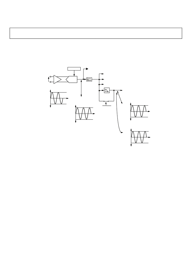
Figure 21 shows the ADC and signal processing chain for the
Voltage Channel. In waveform sampling mode, the ADC
outputs a signed twos complement 24-bit data-word at a
Rev. PrD | Page 44 of 140
maximum of 25.6 kSPS (MCLK/160). The ADC produces an
output code that is approximately between 0x28F5 (+10,485d)
and 0xD70B (–10,485d)—see Figure 22.
x1, x2, x4,
x8, x16
{GAIN[7:5]}
ANALOG
INPUT
RANGE
HPF
ADC
REFERENCE
V2
0V
0.5V, 0.25V,
0.125V, 62.5mV,
31.3mV
WAVEFORM SAMPLE
REGISTER
VOLTAGE RMS (VRMS)
CALCULATION
VP
PGA2
V2
VOLTAGE CHANNEL
WAVEFORM
DATA RANGE
0xD70B
0x
0000
0x28F5
ACTIVE AND REACTIVE
POWER CALCULATION
LPF1
f
–
3dB
= 63.7Hz
MODE1[6]
ZX SIGNAL
DATA RANGE for 60Hz signal
0xE230
0x
0000
0x1DD0
ZX DETECTION
ZX SIGNAL
DATA RANGE for 50Hz signal
0xDFC9
0x
0000
0x2037
VOLTAGE PEAK DETECT
Figure 22. ADC and Signal Processing in Voltage Channel
Channel Sampling
The waveform samples of the current ADC and voltage ADC
can also be routed to the waveform registers to be read by the
MCU core. The active, reactive, apparent power, and energy
calculation remain uninterrupted during waveform sampling.
When in waveform sampling mode, one of four output sample
rates can be chosen by using Bits 0 and 1 of the WAVMODE
register (WAVSEL1,0). The output sample rate can be 25.6 kSPS,
12.8kSPS, 6.4 kSPS, or 3.2 kSPS—see Table 30. If the WFSM
enable bit is set in the Interrupt Enable Register 3 SFR
(MIRQENH, 0xDB), the 8052 core has a pending ADE
interrupt. The sampled signals selected in the WAVMODE
register will be latched into the Waveform SFRs when the
waveform high byte (WAV1H or WAV2H) is read.
The ADE interrupt stays active until the WFSM status bit is
cleared—see Energy measurement interrupts section.
FAULT DETECTION
The ADE7169F16 incorporates a fault detection scheme that
warns of fault conditions and allows the ADE7169F16 to
continue accurate measurement during a fault event. The
ADE7169F16 does this by continuously monitoring both
current inputs (IA and IB). These currents will be referred for
ease of understanding as phase and neutral (return) currents. In
the ADE7169F16, a fault condition is defined when the
difference between I
A
and I
B
is greater than 6.25% of the active
channel. If a fault condition is detected and the inactive channel
is larger than the active channel, the ADE7169F16 automatically
switches to current measurement to the inactive channel.
During a fault, the active, reactive, current rms and apparent
powers are generated using the larger of the two currents. On
power-up, I
A
is the current input selected for Active, Reactive,
and Apparent power and Irms calculations.
To prevent false alarm, averaging is done for the fault detection
and a fault condition is detected approximately 1 second after
the event. The fault detection is automatically disabled when the
voltage signal is less than 0.3% of the full-scale input range. This
eliminates false detection of a fault due to noise at light loads.
Because the ADE7169F16 looks for a difference between the
voltage signals on I
A
and I
B
, it is important that both current
transducers be closely matched.
Channel selection Indication
The current channel selected for measurement is indicated by
bit 7 (ICHANNEL) in the ACCMODE register (0x0F). When
this bit is cleared, I
A
is selected and when it is set, I
B
is selected.
相關(guān)PDF資料 |
PDF描述 |
|---|---|
| ADE7169ACPF16-RL | Single-Phase Energy Measurement IC with 8052 MCU, RTC and LCD driver |
| ADE7169ACPZF16 | Single-Phase Energy Measurement IC with 8052 MCU, RTC and LCD driver |
| ADE7169ACPZF16-RL | Single-Phase Energy Measurement IC with 8052 MCU, RTC and LCD driver |
| ADE7169ASTF16 | Single-Phase Energy Measurement IC with 8052 MCU, RTC and LCD driver |
| ADE7169ASTF16-RL | Single-Phase Energy Measurement IC with 8052 MCU, RTC and LCD driver |
相關(guān)代理商/技術(shù)參數(shù) |
參數(shù)描述 |
|---|---|
| ADE7169ACPF16-RL | 制造商:AD 制造商全稱(chēng):Analog Devices 功能描述:Single-Phase Energy Measurement IC with 8052 MCU, RTC and LCD driver |
| ADE7169ACPZF16 | 制造商:AD 制造商全稱(chēng):Analog Devices 功能描述:Single-Phase Energy Measurement IC with 8052 MCU, RTC, and LCD Driver |
| ADE7169ACPZF161 | 制造商:AD 制造商全稱(chēng):Analog Devices 功能描述:Single-Phase Energy Measurement IC with 8052 MCU, RTC and LCD driver |
| ADE7169ACPZF16-RL | 制造商:AD 制造商全稱(chēng):Analog Devices 功能描述:Single-Phase Energy Measurement IC with 8052 MCU, RTC, and LCD Driver |
| ADE7169ACPZF16-RL1 | 制造商:AD 制造商全稱(chēng):Analog Devices 功能描述:Single-Phase Energy Measurement IC with 8052 MCU, RTC and LCD driver |
發(fā)布緊急采購(gòu),3分鐘左右您將得到回復(fù)。