- 您現(xiàn)在的位置:買賣IC網(wǎng) > PDF目錄375238 > AD7710SQ (ANALOG DEVICES INC) Signal Conditioning ADC PDF資料下載
參數(shù)資料
| 型號(hào): | AD7710SQ |
| 廠商: | ANALOG DEVICES INC |
| 元件分類: | ADC |
| 英文描述: | Signal Conditioning ADC |
| 中文描述: | 2-CH 24-BIT DELTA-SIGMA ADC, SERIAL ACCESS, CDIP24 |
| 封裝: | 0.300 INCH, HERMETIC SEALED, CERDIP-24 |
| 文件頁(yè)數(shù): | 15/28頁(yè) |
| 文件大小: | 220K |
| 代理商: | AD7710SQ |
第1頁(yè)第2頁(yè)第3頁(yè)第4頁(yè)第5頁(yè)第6頁(yè)第7頁(yè)第8頁(yè)第9頁(yè)第10頁(yè)第11頁(yè)第12頁(yè)第13頁(yè)第14頁(yè)當(dāng)前第15頁(yè)第16頁(yè)第17頁(yè)第18頁(yè)第19頁(yè)第20頁(yè)第21頁(yè)第22頁(yè)第23頁(yè)第24頁(yè)第25頁(yè)第26頁(yè)第27頁(yè)第28頁(yè)
AD7710
REV. F
–15–
Antialias Considerations
The digital filter does not provide any rejection at integer mul-
tiples of the modulator sample frequency (n
×
19.5 kHz, where
n = 1, 2, 3 . . . ). This means that there are frequency bands,
±
f
3 dB
wide (f
3 dB
is cutoff frequency selected by FS0 to FS11)
where noise passes unattenuated to the output. However, due to
the AD7710’s high oversampling ratio, these bands occupy only
a small fraction of the spectrum and most broadband noise is
filtered. In any case, because of the high oversampling ratio a
simple, RC, single pole filter is generally sufficient to attenuate
the signals in these bands on the analog input and thus provide
adequate antialiasing filtering.
If passive components are placed in front of the AD7710, care
must be taken to ensure that the source impedance is low enough
so as not to introduce gain errors in the system. The dc input
impedance for the AD7710 is over 1 G
. The input appears as
a dynamic load which varies with the clock frequency and with
the selected gain (see Figure 7). The input sample rate, as
shown in Table III, determines the time allowed for the analog
input capacitor, C
IN
, to be charged. External impedances result
in a longer charge time for this capacitor and this may result
in gain errors being introduced on the analog inputs. Table IV
shows the allowable external resistance/capacitance values such
that no gain error to the 16-bit level is introduced while Table V
shows the allowable external resistance/capacitance values such
that no gain error to the 20-bit level is introduced. Both inputs
of the differential input channels look into similar input circuitry.
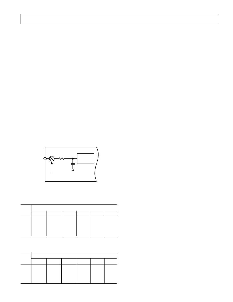
R
INT
7k
V
TYP
C
INT
11.5pF TYP
V
BIAS
AIN
SWITCHING FREQ DEPENDS ON
f
CLKIN
AND SELECTED GAIN
HIGH
IMPEDANCE
>1G
V
AD7710
Figure 7. Analog Input Impedance
Table IV. Typical External Series Resistance That Will Not
Introduce 16-Bit Gain Error
External Capacitance (pF)
Gain
0
184 k
88.6 k
22.1 k
13.2 k
3.6 k
41.4 k
10.6 k
6.3 k
17.6 k
4.8 k
50
45.3 k
27.1 k
7.3 k
100
500
1000
4.1 k
2.0 k
970
440
5000
1.1 k
560
270
120
1
2
4
8–128
1.7 k
790
2.9 k
Table V. Typical External Series Resistance That Will Not
Introduce 20-Bit Gain Error
External Capacitance (pF)
Gain
0
145 k
70.5 k
16.9 k
10 k
31.8 k
8.0 k
13.4 k
3.6 k
50
34.5 k
20.4 k
5.2 k
100
500
1000
2.8 k
1.4 k
670
300
5000
700
350
170
80
1
2
4
8–128
2.5 k
1.2 k
550
4.8 k
2.2 k
The numbers in the above tables assume a full-scale change on
the analog input. In any case, the error introduced due to longer
charging times is a gain error which can be removed using the
system calibration capabilities of the AD7710 provided that the
resultant span is within the span limits of the system calibration
techniques for the AD7710.
ANALOG INPUT FUNCTIONS
Analog Input Ranges
Both analog inputs are differential, programmable gain, input
channels which can handle either unipolar or bipolar input
signals. The common-mode range of these inputs is from V
SS
to
AV
DD
, provided that the absolute value of the analog input
voltage lies between V
SS
–30 mV and AV
DD
+30 mV.
The dc input leakage current is 10 pA maximum at 25
°
C
(
±
1 nA over temperature). This results in a dc offset voltage
developed across the source impedance. However, this dc offset
effect can be compensated for by a combination of the differen-
tial input capability of the part and its system calibration mode.
Burnout Current
The AIN1(+) input of the AD7710 contains a 4.5
μ
A current
source which can be turned on/off via the control register. This
current source can be used in checking that a transducer has not
burned out or gone open circuit before attempting to take mea-
surements on that channel. If the current is turned on and
allowed flow into the transducer and a measurement of the
input voltage on the AIN1 input is taken, it can indicate that the
transducer has burned out or gone open circuit. For normal
operation, this burnout current is turned off by writing a 0 to
the BO bit in the control register.
Output Compensation Current
The AD7710 also contains a feature which can enable the user
to implement cold junction compensation in thermocouple
applications. This can be achieved using the output compensa-
tion current from the I
OUT
pin of the device. Once again, this
current can be turned on/off via the control register. Writing a 1
to the IO bit of the control register enables this compensation
current.
The compensation current provides a 20
μ
A constant current
source which can be used in association with a thermistor or a
diode to provide cold junction compensation. A common
method of generating cold junction compensation is to use a
temperature dependent current flowing through a fixed resistor
to provide a voltage that is equal to the voltage developed across
the cold junction at any temperature in the expected ambient
range. In this case, the temperature coefficient of the compensa-
tion current is so low compared with the temperature coefficient
of the thermistor that it can be considered constant with tem-
perature. The temperature variation is then provided by the
variation of the thermistor’s resistance with temperature.
Normally, the cold junction compensation will be implemented
by applying the compensation voltage to the second input chan-
nel of the AD7710. Periodic conversion of this channel gives the
user a voltage which corresponds to the cold junction compen-
sation voltage. This can be used to implement cold junction
compensation in software with the result from the thermocouple
input being adjusted according to the result in the compensation
channel. Alternatively, the voltage can be subtracted from the
input voltage in an analog fashion, thereby using only one chan-
nel of the AD7710.
相關(guān)PDF資料 |
PDF描述 |
|---|---|
| AD7710* | Signal Conditioning ADC |
| AD7710 | Signal Conditioning ADC(LC2MOS信號(hào)調(diào)節(jié)A/D轉(zhuǎn)換器) |
| AD7711AAR | LC2MOS Signal Conditioning ADC with RTD Current Source |
| AD7711ASQ | LC2MOS Signal Conditioning ADC with RTD Current Source |
| AD7711A* | LC2MOS Signal Conditioning ADC with RTD Current Source |
相關(guān)代理商/技術(shù)參數(shù) |
參數(shù)描述 |
|---|---|
| AD7710SQ/883B | 制造商:未知廠家 制造商全稱:未知廠家 功能描述:Analog-to-Digital Converter, 24-Bit |
| AD7711 | 制造商:AD 制造商全稱:Analog Devices 功能描述:LC2MOS Signal Conditioning ADC with RTD Excitation Currents |
| AD7711A | 制造商:AD 制造商全稱:Analog Devices 功能描述:LC2MOS Signal Conditioning ADC with RTD Current Source |
發(fā)布緊急采購(gòu),3分鐘左右您將得到回復(fù)。