- 您現(xiàn)在的位置:買賣IC網(wǎng) > PDF目錄375235 > AD7011 (Analog Devices, Inc.) CMOS, ADC p/4 DQPSK Baseband Transmit Port PDF資料下載
參數(shù)資料
| 型號(hào): | AD7011 |
| 廠商: | Analog Devices, Inc. |
| 英文描述: | CMOS, ADC p/4 DQPSK Baseband Transmit Port |
| 中文描述: | 的CMOS ADC的p / 4 DQPSK基帶傳輸端口 |
| 文件頁數(shù): | 9/12頁 |
| 文件大小: | 389K |
| 代理商: | AD7011 |
AD7011
REV. B
–9–
I
Q
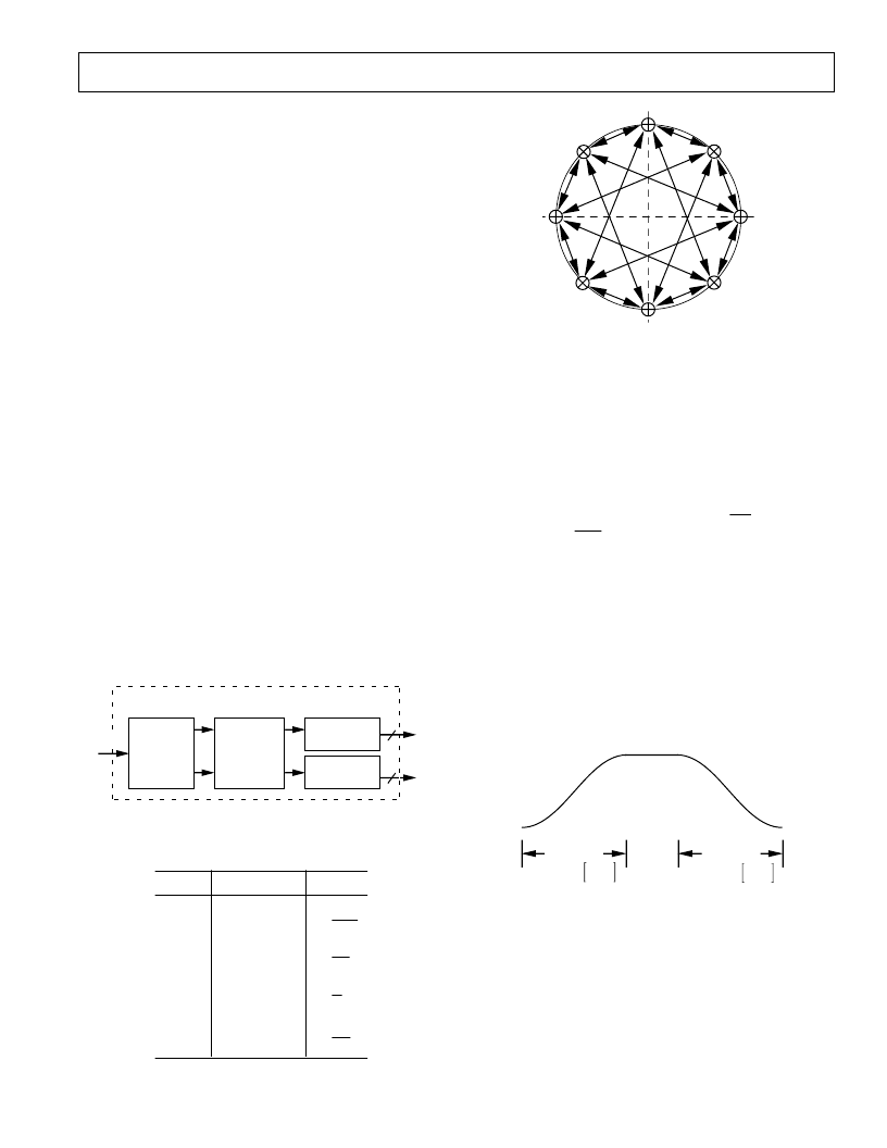
Figure 10.
π
/4 DQPSK Constellation Diagram
Figure 10 illustrates the
π
/4 DQPSK constellation diagram as
described above, showing the eight possible states for [I
k
, Q
k
].
T he I
k
and Q
k
impulses are then filtered by FIR raised root
cosine filters (
α
= 0.35), generating 10-bit I and Q data. T he
FIR root raised cosine filters have an impulse response of
±
4
symbols.
T ransmit Calibration
When the transmit section is brought out of sleep mode
(POWER high), the transmit section initiates a self-calibration
routine to remove the offset between IT x and
ITx
and an offset
between QT x and
QTx
. READY goes high on the completion
of the self-calibration routine. Once READY goes high, BIN
(Burst In) can be brought high to initiate a transmit burst.
Ramp-Up/Down E nvelope Logic
T he AD7011 provides on-chip envelope shaping logic, providing
power shaping control for the beginning and end of a transmit
burst. When BIN (Burst In) is brought high, the modulator is
reset to a transmitting all zeros state (i.e., X
k
= Y
k
= 0) and
continues to transmit all zeros for the first three symbols, during
which the ramp-up envelope goes from zero to full scale as
illustrated in Figure 11. T he next symbol to be transmitted is
[I
1
, Q
1
], which represents the first two data bits clocked in after
BIN going high, i.e., [X
1
, Y
1
].
2
π
–––
2
1
1
t
3T
2
π
–––
2
1
1
t
3T
3 SYMBOLS
3 SYMBOLS
Figure 11. Ramp Envelope
When BIN is brought low, indicating the end of a transmit
burst, the current Di-bit symbol [X
N+4
, Y
N+4
] that the AD7011
is receiving will be the last symbol to be computed for the four
symbol ramp-down sequence. Also the N
th
symbol is the last
active symbol prior to ramping down.
However, because the impulse response is equal to
±
4 symbols,
four additional symbols are required to fully compute the analog
outputs when transmitting the (N+4)
th
symbol. Hence there will
be eight subsequent T xCLK s, latching four additional Di-bit
symbols: [X
N + 5
, Y
N + 5
] to [X
N + 8
, Y
N + 8
].
CIRCUIT DE SCRIPT ION
T RANSMIT SE CT ION
T he transmit section of the AD7011 generates
π
/4 DQPSK I
and Q waveforms in accordance with T IA specification. T his is
accomplished by a digital
π
/4 DQPSK modulator, which
includes the root-raised cosine filters (
α
= 0.35), followed by
two 10-bit DACs and on-chip reconstruction filters. T he
π
/4
DQPSK (Differential Quadrature Phase Shift K eying) digital
modulator generates 10-bit I and Q data in response to the
transmit data stream. T he 10-bit I and Q DACs are filtered by
on-chip reconstruction filters, which also generate differential
analog outputs for both I and Q channels.
T he AD7011 transmit channel also provides an analog mode,
where direct access to the I and Q DACs is provided, bypassing
the
π
/4 DQPSK modulator. T his is provided so that the
AD7011 transmit channel can also be used to perform the
conversion and filtering of the analog waveforms required to
emulate the existing analog cellular system.
p
/4 DQPSK Modulator
T he
π
/4 DQPSK modulator generates 10-bit I and Q data
(Inphase and Quadrature) which are loaded into the I and Q
10-bit transmit DACs.
Figure 9 shows the functional block diagram of the
π
/4 DQPSK
modulator. T he transmit serial data (T xDAT A) is first con-
verted into Di-bit symbols [X
k
, Y
k
], using a 2-bit serial to parallel
converter. T he data is then differentially encoded; symbols are
transmitted as changes in phase rather than absolute phases.
Each symbol represents a phase change, as illustrated in T able
III, and this along with the previously transmitted symbol
determines the next symbol to be transmitted. T he differential
phase encoder generates I and Q impulses [I
k
, Q
k
] in response to
the Di-bit symbols according to:
I
k
= COS
[
φ
k–
1
+
φ
k
]
Q
k
= SIN
[
φ
k–
1
+
φ
k
]
AAAAAAAAA
X
k
DIFFERENTIAL
PHASE
ENCODER
ROOT-RAISED
COSINE FILTER
Q DATA
10
10
2-BIT
PARALLEL
AAAAAAAAA
Figure 9.
π
/4 DQPSK Modulator Functional Block Diagram
AAAAAAAAA
TxDATA
π
/4 DQPSK DIGITAL
Y
k
I
k
Q
k
ROOT-RAISED
COSINE FILTER
T able III.
X
k
Y
k
f
k
1
1
3
π
4
3
π
4
π
4
π
4
0
1
0
0
1
0
相關(guān)PDF資料 |
PDF描述 |
|---|---|
| AD7011ARS | MB 4C 4#12 PIN RECP |
| AD7013ARS | CMOS TIA IS-54 Baseband Receive Port |
| AD7013 | CMOS TIA IS-54 Baseband Receive Port(CMOS 基帶接收口) |
| AD7015 | Complete 3 V GSM/DCS1800 Codec(GSM/DCS1800 編碼譯碼器) |
| AD704AN | Quad Picoampere Input Current Bipolar Op Amp |
相關(guān)代理商/技術(shù)參數(shù) |
參數(shù)描述 |
|---|---|
| AD7011ARS | 制造商:Analog Devices 功能描述:Quadrature Mod 24-Pin SSOP |
| AD7011ARS-REEL | 制造商:Analog Devices 功能描述:Quadrature Mod 24-Pin SSOP T/R 制造商:Rochester Electronics LLC 功能描述:- Tape and Reel |
| AD7013 | 制造商:AD 制造商全稱:Analog Devices 功能描述:CMOS TIA IS-54 Baseband Receive Port |
| AD7013ARS | 制造商:AD 制造商全稱:Analog Devices 功能描述:CMOS TIA IS-54 Baseband Receive Port |
| AD7013ARS-REEL | 制造商:未知廠家 制造商全稱:未知廠家 功能描述:RF/Baseband Circuit |
發(fā)布緊急采購,3分鐘左右您將得到回復(fù)。