- 您現(xiàn)在的位置:買賣IC網(wǎng) > PDF目錄375235 > AD6816 (Analog Devices, Inc.) Interface For ATM User-Network Interface IC to Category #5 Unshielded Twisted Pair (UTP) system or a fiber optic system.(ATM用戶網(wǎng)絡(luò)接口與#5類非屏蔽雙絞線系統(tǒng)或其他光纖系統(tǒng)的接口芯片) PDF資料下載
參數(shù)資料
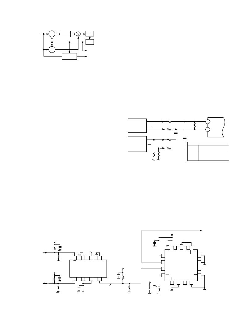
| 型號: | AD6816 |
| 廠商: | Analog Devices, Inc. |
| 英文描述: | Interface For ATM User-Network Interface IC to Category #5 Unshielded Twisted Pair (UTP) system or a fiber optic system.(ATM用戶網(wǎng)絡(luò)接口與#5類非屏蔽雙絞線系統(tǒng)或其他光纖系統(tǒng)的接口芯片) |
| 文件頁數(shù): | 10/20頁 |
| 文件大小: | 483K |
| 代理商: | AD6816 |
AD6816
–10–
REV. A
APPLICATIONS
Application with Fiber Optic Receivers/Transceivers
The AD6816 receiver (adaptive equalizer and baseline restore
loop) can be configured to receive a signal from a fiber optic
receiver or transceiver that provides full PECL or ECL outputs.
By properly adjusting the common mode and amplitude level,
the AD6816 receiver will be essentially transparent to the
(P)ECL inputs. The common-mode input voltage should be
between 1.5 V and 1.9 V referred to V
CC
. The differential input
amplitude should be between 0.7 V and 1.1 V. The common-
mode issue can be addressed simply by ac coupling. The ampli-
tude of the (P)ECL signal should be attenuated by two to meet
the above requirement.
Figure 18 provides a simple solution that satisfies the above
requirements as well as providing proper 50
terminations for
transmission lines when needed. The circuit also allows a conve-
nient way to double pad a PC board for either fiber or copper
cable applications.
PULSE
PE-68517
MAGNETICS
16
15
HP
HFBR5205
OPTICAL
TRANSCEIVER
RD
RD
RD
RD
R7
270
R6
270
C1
10nF
C2
10nF
R4 50
R5 50
R2 0
R1 0
R3
100
AD6816
43
44
RX
RXN
APPLICATION
UTP
OPTICAL
DISMOUNT CAPACITORS
DISCONNECT 0
RESISTORS
R1 AND R2, MOUNT
CAPACITORS C1 AND C2.
Figure 18. Fiber Optic Receiver PECL/ECL Output
Interface to AD6816 Receiver Schematic
Generation of 19.44 MHz TTL-Level Byte Clock from
155.52 MHz Recovered Clock
Some applications require that a local master clock at 19.44 MHz
be generated from the 155.52 MHz recovered clock. Figure 19
shows a circuit schematic for such an application. The circuit
uses one ECL (PECL) IC to divide the recovered 155 MHz clock
by eight, and one ECL/TTL converter IC to deliver the
19.44 MHz TTL output.
1
s
VCO
τ
s +1
F
DET
Φ
DET
FROM
EQUALIZER
AND ZERO
RESTORATION
RECOVERED CLOCK
OUTPUT
RETIMED DATA
OUTPUT
RETIMING
DEVICE
Figure 17. PLL Block Diagram
Jitter caused by variations of density of data transitions (pattern
jitter) is virtually eliminated by use of a new phase detector
(patented). Briefly, the measurement of zero phase error does
not cause the VCO phase to increase to above the average run
rate set by the data frequency. The jitter created by a 2
7
-1
pseudo random code is 1/2 degree; this is small compared to
random jitter.
The jitter bandwidth for the PLL is 0.07% of the center fre-
quency. This figure is chosen so that sinusoidal input jitter at
110 kHz will be attenuated by 3 dB.
The damping ratio of the PLL is user programmable with a
single external capacitor. At 155 MHz, a damping ratio of 5 is
obtained with a 0.15
μ
F capacitor. More generally, the damping
ratio scales as (
f
DATA
×
C
D
)
1/2
.
A lower damping ratio allows a faster frequency acquisition;
generally the acquisition time scales directly with the capacitor
value. However, at damping ratios approaching one, the acquisi-
tion time no longer scales directly with capacitor value. The ac-
quisition time has two components: frequency acquisition and
phase acquisition. The frequency acquisition always scales with
capacitance, but the phase acquisition is set by the loop band-
width of the PLL and is independent of the damping ratio.
Thus, the 0.07% fractional loop bandwidth sets a minimum ac-
quisition time of 2000 bit periods. Note the acquisition time for
a damping factor of one 15,000 bit periods. This comprises
13,000 bit periods for frequency acquisition and 2,000 bit peri-
ods for phase acquisition. Compare this to the 400,000 bit peri-
ods acquisition time for a damping ratio of 5; this consists
entirely of frequency acquisition, and the 2,000 bit periods of
phase acquisition is negligible.
While a lower damping ratio affords faster acquisition, it also al-
lows more peaking in the jitter transfer response (jitter peaking).
For example, with a damping ratio of 10 the jitter peaking is
0.02 dB, but with a damping ratio of 1, the peaking is 2 dB.
8
7
6
5
IN
NC
MC
GND
IN
V
CC
SW
3
OUT
C7
0.1μF
+5V
19.44 MHz
TTL CLOCK
C5
0.1μF
+5V
+5V
+5V
+5V
R2
130
RCLKOUT
(PIN 10)
RCLKOUTN
(PIN 11)
R5
80
R6
R7
80
R8
DIN
DIN
DOUT
OE
ECL
V
CC
AOUT
AIN
AIN
RXCLKOUT
DBY 8
T
V
C
C
C
C
B
B
B
G
8
5
6
7
13
16
15
14
12
11
10
9
2
3
4
1
Z2
MC10H350
ECL TO TTL
TRANSLATOR
C6
0.1μF
Z1
MC12026A or B
1.1 GHz
MODULATOR PRESCALAR
2
1
4
C4
0.1μF
+5V
C3
0.1μF
C1
R1
80
+5V
R4
130
C2
R3
80
Figure 19. Generation of 19.44 MHz TTL-Level Byte Clock from 155.52 MHz Recovered Clock-Circuit Schematic
相關(guān)PDF資料 |
PDF描述 |
|---|---|
| AD693(中文) | Loop-Powered 4-20 mA Sensor Transmitter(環(huán)路供電,4-20mA傳感器變送器) |
| AD7010ARS | MIL-spec connector accessory |
| AD7010 | CMOS JDC DQPSK Baseband Transmit Port(CMOS 基帶傳輸口) |
| AD7011 | CMOS, ADC p/4 DQPSK Baseband Transmit Port |
| AD7011ARS | MB 4C 4#12 PIN RECP |
相關(guān)代理商/技術(shù)參數(shù) |
參數(shù)描述 |
|---|---|
| AD6816KST | 制造商:Rochester Electronics LLC 功能描述:- Tape and Reel |
| AD681AQ | 制造商:未知廠家 制造商全稱:未知廠家 功能描述:Sample/Track-and-Hold Amplifier |
| AD681SQ | 制造商:未知廠家 制造商全稱:未知廠家 功能描述:Sample/Track-and-Hold Amplifier |
| AD682AN | 制造商:未知廠家 制造商全稱:未知廠家 功能描述:Sample/Track-and-Hold Amplifier |
| AD682JN | 制造商:未知廠家 制造商全稱:未知廠家 功能描述:Sample/Track-and-Hold Amplifier |
發(fā)布緊急采購,3分鐘左右您將得到回復(fù)。