- 您現(xiàn)在的位置:買賣IC網(wǎng) > PDF目錄11674 > AD2S90APZ (Analog Devices Inc)IC R/D CONV 12BIT 20-PLCC PDF資料下載
參數(shù)資料
| 型號(hào): | AD2S90APZ |
| 廠商: | Analog Devices Inc |
| 文件頁(yè)數(shù): | 7/12頁(yè) |
| 文件大小: | 0K |
| 描述: | IC R/D CONV 12BIT 20-PLCC |
| 標(biāo)準(zhǔn)包裝: | 1 |
| 類型: | R/D 轉(zhuǎn)換器 |
| 輸入類型: | 并聯(lián) |
| 輸出類型: | 數(shù)字 |
| 接口: | 串行 |
| 電流 - 電源: | 10mA |
| 安裝類型: | 表面貼裝 |
| 封裝/外殼: | 20-LCC(J 形引線) |
| 供應(yīng)商設(shè)備封裝: | 20-PLCC(9x9) |
| 包裝: | 管件 |
| 產(chǎn)品目錄頁(yè)面: | 790 (CN2011-ZH PDF) |
AD2S90
REV. D
–4–
RECOMMENDED OPERATING CONDITIONS
Power Supply Voltage (VDD – VSS) . . . . . . . . . .
±5 V dc ± 5%
Analog Input Voltage (SIN, COS & REF) . . . . . 2 V rms
± 10%
Signal and Reference Harmonic Distortion . . . . . . . . . . . . 10%
Phase Shift between Signal and Reference . . . . . . . . . . . . .
±10°
Ambient Operating Temperature Range
Industrial (AP) . . . . . . . . . . . . . . . . . . . . . . . –40
°C to +85°C
ABSOLUTE MAXIMUM RATINGS*
VDD to AGND . . . . . . . . . . . . . . . . . . . . –0.3 V dc to +7.0 V dc
VSS to AGND . . . . . . . . . . . . . . . . . . . . +0.3 V dc to –7.0 V dc
AGND to DGND . . . . . . . . . . . . –0.3 V dc to VDD + 0.3 V dc
Analog Inputs to AGND
REF . . . . . . . . . . . . . . . . . . VSS – 0.3 V dc to VDD + 0.3 V dc
SIN, SIN LO . . . . . . . . . . . VSS – 0.3 V dc to VDD + 0.3 V dc
COS, COS LO . . . . . . . . . . VSS – 0.3 V dc to VDD + 0.3 V dc
Analog Output to AGND
VEL . . . . . . . . . . . . . . . . . . . . . . . . . . . . . . . . . . . VSS to VDD
Digital Inputs to DGND, CSB,
SCLK, RES . . . . . . . . . . . . . . . –0.3 V dc to VDD + 0.3 V dc
Digital Outputs to DGND, NM, A, B,
DIR, CLKOUT DATA . . . . . . –0.3 V dc to VDD + 0.3 V dc
Operating Temperature Range
Industrial (AP) . . . . . . . . . . . . . . . . . . . . . . . –40
°C to +85°C
Storage Temperature Range . . . . . . . . . . . . . –65
°C to +150°C
Lead Temperature (Soldering 10 sec) . . . . . . . . . . . . . . 300
°C
Power Dissipation to +75
°C . . . . . . . . . . . . . . . . . . . . 300 mW
Derates above +75
°C by . . . . . . . . . . . . . . . . . . . . . 10 mW/°C
*Stresses above those listed under Absolute Maximum Ratings may cause perma-
nent damage to the device. This is a stress rating only; functional operation of the
device at these or any other conditions above those indicated in the operational
section of this specification is not implied. Exposure to absolute maximum rating
conditions for extended periods may affect device reliability.
ORDERING GUIDE
Model
Temperature Range Accuracy
Package Option
AD2S90AP –40
°C to +85°C
10.6 arc min P-20A
CAUTION
The AD2S90 features an input protection circuit consisting of large “distributed” diodes and
polysilicon series resistors to dissipate both high energy discharges (Human Body Model) and
fast, low energy pulses (Charges Device Model).
Proper ESD precautions are strongly recommended to avoid functional damage or performance
degradation. For further information on ESD precautions, refer to Analog Devices ESD
Prevention Manual.
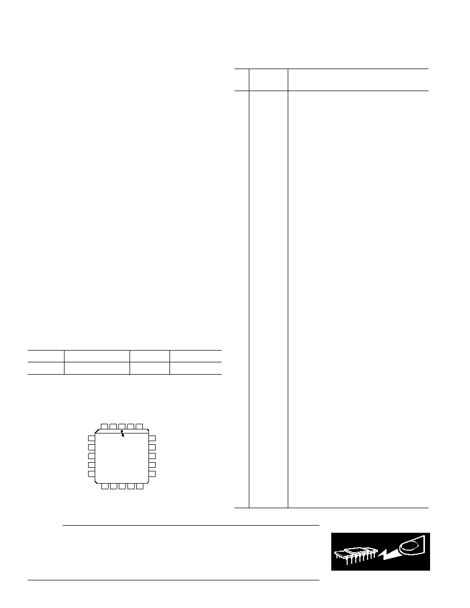
PIN DESCRIPTIONS
Pin
No. Mnemonic Function
1
AGND
Analog ground, reference ground.
2
SIN
SIN channel noninverting input connect to
resolver SIN HI output. SIN to SIN LO =
2 V rms
± 10%.
3
SIN LO
SIN channel inverting input connect to
resolver SIN LO.
4
DATA
Serial interface data output. High impedance
with
CS = HI. Enabled by CS = 0.
5
SCLK
Serial interface clock. Data is clocked out on
“first” negative edge of SCLK after a LO transi-
tion on
CS. 12 SCLK pulses to clock data out.
6
CS
Chip select. Active LO. Logic LO transition
enables DATA output.
7
A
Encoder A output.
8
B
Encoder B output.
9
NM
Encoder North Marker emulation output.
Pulse triggered as code passes through zero.
Three common pulsewidths available.
10
DIR
Indicates direction of rotation of input.
Logic HI = increasing angular rotation.
Logic LO = decreasing angular rotation.
11
DGND
Digital power ground return.
12
VSS
Negative power supply, –5 V dc
± 5%.
13
VDD
Positive power supply, +5 V dc
± 5%.
14
VDD
Positive power supply, +5 V dc
± 5%. Must
be connected to Pin 13.
15
NMC
North marker width control. Internally pulled
HI via 50 k
nominal.
16
CLKOUT
Internal VCO clock output. Indicates angular
velocity of input signals. Max nominal rate =
1.536 MHz. CLKOUT is a 300 ns positive pulse.
17
VEL
Indicates angular velocity of input signals.
Positive voltage w.r.t. AGND indicates in-
creasing angle. FSD = 375 rps.
18
REF
Converter reference input. Normally derived
from resolver primary excitation. REF = 2 V
rms nominal. Phase shift w.r.t. COS and SIN
=
±10° max
19
COS LO
COS channel inverting input. Connect to
resolver COS LO.
20
COS
COS channel noninverting input. Connect to
resolver COS HI output. COS = 2 V rms
± 10%.
3
2
1
20
19
9
10
11
12
13
18
17
16
15
14
4
5
6
7
8
TOP VIEW
(Not to Scale)
PIN 1
IDENTIFIER
DATA
SCLK
CS
A
B
REF
VEL
CLKOUT
NMC
VDD
AD2S90
SIN
LO
SIN
AGND
COS
LO
NM
DIR
DGND
V
SS
V
DD
WARNING!
ESD SENSITIVE DEVICE
PIN CONFIGURATION
相關(guān)PDF資料 |
PDF描述 |
|---|---|
| 226990-3 | CONN JACK BNC RT/A 50OHM PCB AU |
| AD598JRZ | IC LVDT SGNL COND OSC/REF 20SOIC |
| 221185-2 | CONN PLUG BNC 75 OHM DUAL CRIMP |
| AD698APZ | IC LVDT SIGNAL COND 28-PLCC |
| 221185-8 | CONN PLUG BNC 75 OHM DUAL CRIMP |
相關(guān)代理商/技術(shù)參數(shù) |
參數(shù)描述 |
|---|---|
| AD2S90APZ-MOOG | 制造商:Analog Devices 功能描述: |
| AD2S90APZ-RL7 | 功能描述:IC R/D CONV 12BIT 20-PLCC 制造商:analog devices inc. 系列:* 零件狀態(tài):在售 標(biāo)準(zhǔn)包裝:250 |
| AD2S90-EB | 制造商:Analog Devices 功能描述:EVALUATION BOARD - Bulk |
| AD2S93 | 制造商:AD 制造商全稱:Analog Devices 功能描述:Low Cost LVDT-to-Digital Converter |
| AD2S93AP | 制造商:AD 制造商全稱:Analog Devices 功能描述:Low Cost LVDT-to-Digital Converter |
發(fā)布緊急采購(gòu),3分鐘左右您將得到回復(fù)。