- 您現(xiàn)在的位置:買賣IC網(wǎng) > PDF目錄164971 > A3PE1500-PQG208 FPGA, 38400 CLBS, 1500000 GATES, PQFP208 PDF資料下載
參數(shù)資料
| 型號: | A3PE1500-PQG208 |
| 元件分類: | FPGA |
| 英文描述: | FPGA, 38400 CLBS, 1500000 GATES, PQFP208 |
| 封裝: | 28 X 28 MM, 3.40 MM HEIGHT, 0.50 MM PITCH, GREEN, PLASTIC, QFP-208 |
| 文件頁數(shù): | 61/152頁 |
| 文件大?。?/td> | 4932K |
| 代理商: | A3PE1500-PQG208 |
第1頁第2頁第3頁第4頁第5頁第6頁第7頁第8頁第9頁第10頁第11頁第12頁第13頁第14頁第15頁第16頁第17頁第18頁第19頁第20頁第21頁第22頁第23頁第24頁第25頁第26頁第27頁第28頁第29頁第30頁第31頁第32頁第33頁第34頁第35頁第36頁第37頁第38頁第39頁第40頁第41頁第42頁第43頁第44頁第45頁第46頁第47頁第48頁第49頁第50頁第51頁第52頁第53頁第54頁第55頁第56頁第57頁第58頁第59頁第60頁當(dāng)前第61頁第62頁第63頁第64頁第65頁第66頁第67頁第68頁第69頁第70頁第71頁第72頁第73頁第74頁第75頁第76頁第77頁第78頁第79頁第80頁第81頁第82頁第83頁第84頁第85頁第86頁第87頁第88頁第89頁第90頁第91頁第92頁第93頁第94頁第95頁第96頁第97頁第98頁第99頁第100頁第101頁第102頁第103頁第104頁第105頁第106頁第107頁第108頁第109頁第110頁第111頁第112頁第113頁第114頁第115頁第116頁第117頁第118頁第119頁第120頁第121頁第122頁第123頁第124頁第125頁第126頁第127頁第128頁第129頁第130頁第131頁第132頁第133頁第134頁第135頁第136頁第137頁第138頁第139頁第140頁第141頁第142頁第143頁第144頁第145頁第146頁第147頁第148頁第149頁第150頁第151頁第152頁
ProASIC3E DC and Switching Characteristics
2- 4
v1.2
PLL Behavior at Brownout Condition
Actel recommends using monotonic power supplies or voltage regulators to ensure proper
power-up behavior. Power ramp-up should be monotonic at least until VCC and VCCPLXL exceed
brownout activation levels. The VCC activation level is specified as 1.1 V worst-case (see Figure 2-1
on page 2-4 for more details).
When PLL power supply voltage and/or VCC levels drop below the VCC brownout levels (0.75 V ±
0.25 V), the PLL output lock signal goes low and/or the output clock is lost. Refer to the
Power-Up/-Down Behavior of Low-Power Flash Devices chapter of the handbook for information
on clock and lock recovery.
Internal Power-Up Activation Sequence
1. Core
2. Input buffers
3. Output buffers, after 200 ns delay from input buffer activation
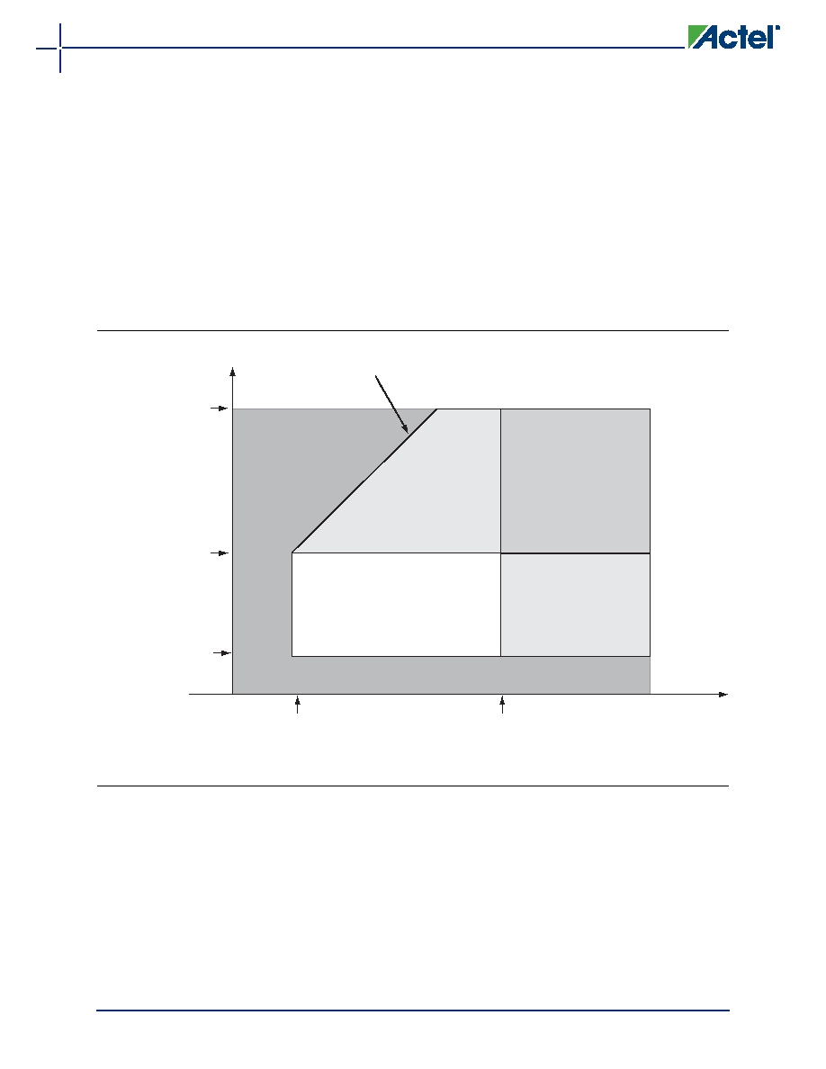
Figure 2-1 I/O State as a Function of VCCI and VCC Voltage Levels
Region 1: I/O buffers are OFF
Region 2: I/O buffers are ON.
I/Os are functional (except differential inputs)
but slower because V
CCI
/V
CC
are below
specification. For the same reason, input
buffers do not meet V
IH
/V
IL
levels, and
output buffers do not meet V
OH
/V
OL
levels.
Min V
CCI datasheet specification
voltage at a selected I/O
standard; i.e., 1.425 V or 1.7 V
or 2.3 V or 3.0 V
VCC
VCC = 1.425 V
Region 1: I/O Buffers are OFF
Activation trip point:
Va = 0.85 V ± 0.25 V
Deactivation trip point:
Vd = 0.75 V ± 0.25 V
Activation trip point:
Va = 0.9 V ± 0.3 V
Deactivation trip point:
Vd = 0.8 V ± 0.3 V
VCC = 1.575 V
Region 5: I/O buffers are ON
and power supplies are within
specification.
I/Os meet the entire datasheet
and timer specifications for
speed, V
IH
/V
IL
, V
OH
/V
OL
, etc.
Region 4: I/O
buffers are ON.
I/Os are functional
(except differential
but slower because V
CCI is
below specification. For the
same reason, input buffers do not
meet V
IH
/V
IL
levels, and output
buffers do not meet V
OH
/V
OL
levels.
Region 4: I/O
buffers are ON.
I/Os are functional
(except differential inputs)
where VT can be from 0.58 V to 0.9 V (typically 0.75 V)
VCCI
Region 3: I/O buffers are ON.
I/Os are functional; I/O DC
specifications are met,
but I/Os are slower because
the V
CC
is below specification.
V
CC = VCCI + VT
相關(guān)PDF資料 |
PDF描述 |
|---|---|
| A3PN060-FVQ100 | FPGA, 1536 CLBS, 60000 GATES, PQFP100 |
| A3PN060-FVQG100 | FPGA, 1536 CLBS, 60000 GATES, PQFP100 |
| A3PN060-ZFVQ100 | FPGA, 1536 CLBS, 60000 GATES, PQFP100 |
| A3PN060-ZFVQG100 | FPGA, 1536 CLBS, 60000 GATES, PQFP100 |
| A3PN125-FVQ100 | FPGA, 3072 CLBS, 125000 GATES, PQFP100 |
相關(guān)代理商/技術(shù)參數(shù) |
參數(shù)描述 |
|---|---|
| A3PE1500-PQG208I | 功能描述:IC FPGA 1KB FLASH 1.5M 208-PQFP RoHS:是 類別:集成電路 (IC) >> 嵌入式 - FPGA(現(xiàn)場可編程門陣列) 系列:ProASIC3E 產(chǎn)品培訓(xùn)模塊:Three Reasons to Use FPGA's in Industrial Designs Cyclone IV FPGA Family Overview 特色產(chǎn)品:Cyclone? IV FPGAs 標(biāo)準(zhǔn)包裝:60 系列:CYCLONE® IV GX LAB/CLB數(shù):9360 邏輯元件/單元數(shù):149760 RAM 位總計(jì):6635520 輸入/輸出數(shù):270 門數(shù):- 電源電壓:1.16 V ~ 1.24 V 安裝類型:表面貼裝 工作溫度:0°C ~ 85°C 封裝/外殼:484-BGA 供應(yīng)商設(shè)備封裝:484-FBGA(23x23) |
| A3PE1500-PQG896 | 制造商:ACTEL 制造商全稱:Actel Corporation 功能描述:ProASIC3E Flash Family FPGAs |
| A3PE1500-PQG896ES | 制造商:ACTEL 制造商全稱:Actel Corporation 功能描述:ProASIC3E Flash Family FPGAs |
| A3PE1500-PQG896I | 制造商:ACTEL 制造商全稱:Actel Corporation 功能描述:ProASIC3E Flash Family FPGAs |
| A3PE1500-PQG896PP | 制造商:ACTEL 制造商全稱:Actel Corporation 功能描述:ProASIC3E Flash Family FPGAs |
發(fā)布緊急采購,3分鐘左右您將得到回復(fù)。