- 您現(xiàn)在的位置:買賣IC網(wǎng) > PDF目錄294128 > 72V805L15PFI9 (INTEGRATED DEVICE TECHNOLOGY INC) 256 X 18 BI-DIRECTIONAL FIFO, 10 ns, PQFP128 PDF資料下載
參數(shù)資料
| 型號: | 72V805L15PFI9 |
| 廠商: | INTEGRATED DEVICE TECHNOLOGY INC |
| 元件分類: | FIFO |
| 英文描述: | 256 X 18 BI-DIRECTIONAL FIFO, 10 ns, PQFP128 |
| 封裝: | TQFP-128 |
| 文件頁數(shù): | 24/26頁 |
| 文件大?。?/td> | 325K |
| 代理商: | 72V805L15PFI9 |
第1頁第2頁第3頁第4頁第5頁第6頁第7頁第8頁第9頁第10頁第11頁第12頁第13頁第14頁第15頁第16頁第17頁第18頁第19頁第20頁第21頁第22頁第23頁當(dāng)前第24頁第25頁第26頁
IDT72V805/72V815/72V825/72V835/72V845
3.3 V CMOS DUAL SyncFIFO 256 x 18, 512 x 18, 1,024 x 18, 4,096 x 18
COMMERCIAL AND INDUSTRIAL
TEMPERATURE RANGES
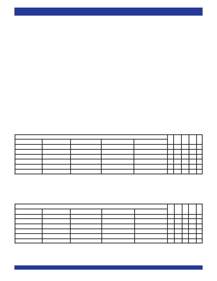
7
Number of Words in FIFO
IDT72V805
IDT72V815
IDT72V825
IDT72V835
IDT72V845
IR PAF HF PAE OR
0
L
H
HLH
1 to (n + 1)(1)
LH
HL
L
(n + 2) to 129
(n + 2) to 257
(n + 2) to 513
(n + 2) to 1,025
(n + 2) to 2,049
L
H
L
130 to (257-(m+1))(2)
258 to (513-(m+1))(2)
514 to (1,025-(m+1))(2)
1,026 to (2,049-(m+1))(2)
2,050 to (4,097-(m+1))(2)
LHL
HL
(257-m) to 256
(513-m) to 512
(1,025-m) to 1,024
(2,049-m) to 2,048
(4,097-m) to 4,096
LLL
H
L
257
513
1,025
2,049
4,097
H
L
H
L
normal read/write operation. When the
LD pin and WEN are again set LOW,
the next offset register in sequence is written.
The contents of the offset registers can be read on the data output lines
Q0-Q11 when the
LD pin is set LOW and REN is set LOW. Data can then
be read on the next LOW-to-HIGH transition of RCLK. The first transition
of RCLK will present the Empty Offset value to the data output lines. The
next transition of RCLK will present the Full Offset value. Offset register
content can be read out in the IDT Standard mode only. It cannot be read
in the FWFT mode.
SYNCHRONOUS VS ASYNCHRONOUS PROGRAMMABLE FLAG
TIMING SELECTION
The IDT72V805/72V815/72V825/72V835/72V845 can be configured
during the "Configuration at Reset" cycle described in Table 3 with either
asynchronous or synchronous timing for
PAE and PAF flags.
If asynchronous
PAE/PAF configuration is selected (as per Table 3), the
PAE is asserted LOW on the LOW-to-HIGH transition of RCLK. PAE is reset
to HIGH on the LOW-to-HIGH transition of WCLK. Similarly, the
PAF is
asserted LOW on the LOW-to-HIGH transition of WCLK and
PAF is reset
to HIGH on the LOW-to-HIGH transition of RCLK. For detail timing dia-
grams, see Figure 13 for asynchronous
PAE timing and Figure 14 for
asynchronous
PAF timing.
If synchronous
PAE/PAF configuration is selected , the PAE is asserted
and updated on the rising edge of RCLK only and not WCLK. Similarly,
PAF
is asserted and updated on the rising edge of WCLK only and not RCLK. For
detail timing diagrams, see Figure 22 for synchronous
PAE timing and
Figure 23 for synchronous
PAF timing.
REGISTER-BUFFERED FLAG OUTPUT SELECTION
The IDT72V805/72V815/72V825/72V835/72V845 can be configured
during the "Configuration at Reset" cycle described in Table 4 with single,
double or triple register-buffered flag output signals. The various combina-
tions available are described in Table 4 and Table 5. In general, going from
single to double or triple buffered flag outputs removes the possibility of
metastable flag indications on boundary states (i.e, empty or full condi-
tions). The trade-off is the addition of clock cycle delays for the respective
flag to be asserted. Not all combinations of register-buffered flag outputs
are supported. Register-buffered outputs apply to the Empty Flag and Full
Flag only. Partial flags are not effected. Table 4 and Table 5 summarize
the options available.
TABLE 1 — STATUS FLAGS FOR IDT STANDARD MODE
Number of Words in FIFO
IDT72V805
IDT72V815
IDT72V825
IDT72V835
IDT72V845
FF PAF
HF PAE EF
00
0
H
L
1 to n(1)
HH
H
L
H
(n + 1) to 128
(n + 1) to 256
(n + 1) to 512
(n + 1) to 1,024
(n + 1) to 2,048
H
129 to (256-(m+1))(2)
257 to (512-(m+1))(2)
513 to (1,024-(m+1))(2)
1,025 to (2,048-(m+1))(2)
2,049 to (4,096-(m+1))(2)
HH
L
H
(256-m) to 255
(512-m) to 511
(1,024-m) to 1,023
(2,048-m) to 2,047
(4,096-m) to 4,095
H
L
H
256
512
1,024
2,048
4,096
L
H
TABLE 2 — STATUS FLAGS FOR FWFT MODE
NOTES:
1. n = Empty Offset (Default Values : IDT72V805 n=31, IDT72V815 n = 63, IDT72V825/72V835/72V845 n = 127)
2. m = Full Offset (Default Values : IDT72V805 m=31, IDT72V815 m = 63, IDT72V825/72V835/72V845 m = 127)
NOTES:
1. n = Empty Offset (Default Values : IDT72V805 n = 31, IDT72V815 n = 63, IDT72V825/72V835/72V845 n = 127)
2. m = Full Offset (Default Values : IDT72V805 m = 31, IDT72V815 m = 63, IDT72V825/72V835/72V845 m = 127)
相關(guān)PDF資料 |
PDF描述 |
|---|---|
| 72V805L15PF8 | 256 X 18 BI-DIRECTIONAL FIFO, 10 ns, PQFP128 |
| 7305-0-15-15-47-14-04-0 | BRASS, GOLD FINISH, PCB TERMINAL |
| 7305-0-15-15-47-01-04-0 | BRASS, GOLD FINISH, PCB TERMINAL |
| 7305-0-15-01-47-27-04-0 | BRASS, TIN FINISH, PCB TERMINAL |
| 7305-0-15-01-47-14-04-0 | BRASS, TIN FINISH, PCB TERMINAL |
相關(guān)代理商/技術(shù)參數(shù) |
參數(shù)描述 |
|---|---|
| 72V805L20PF | 功能描述:先進(jìn)先出 RoHS:否 制造商:IDT 電路數(shù)量: 數(shù)據(jù)總線寬度:18 bit 總線定向:Unidirectional 存儲容量:4 Mbit 定時類型:Synchronous 組織:256 K x 18 最大時鐘頻率:100 MHz 訪問時間:10 ns 電源電壓-最大:3.6 V 電源電壓-最小:6 V 最大工作電流:35 mA 最大工作溫度:+ 85 C 封裝 / 箱體:TQFP-80 封裝: |
| 72V805L20PF8 | 制造商:Integrated Device Technology Inc 功能描述:FIFO Mem Sync Quad Depth/Width Bi-Dir 256 x 18 x 2 128-Pin TQFP T/R 制造商:Integrated Device Technology Inc 功能描述:FIFO SYNC QUAD DEPTH/WIDTH BI-DIR 256 X 18 X 2 128TQFP - Tape and Reel |
| 72V811L10PF | 功能描述:先進(jìn)先出 RoHS:否 制造商:IDT 電路數(shù)量: 數(shù)據(jù)總線寬度:18 bit 總線定向:Unidirectional 存儲容量:4 Mbit 定時類型:Synchronous 組織:256 K x 18 最大時鐘頻率:100 MHz 訪問時間:10 ns 電源電壓-最大:3.6 V 電源電壓-最小:6 V 最大工作電流:35 mA 最大工作溫度:+ 85 C 封裝 / 箱體:TQFP-80 封裝: |
| 72V811L10PF8 | 功能描述:先進(jìn)先出 RoHS:否 制造商:IDT 電路數(shù)量: 數(shù)據(jù)總線寬度:18 bit 總線定向:Unidirectional 存儲容量:4 Mbit 定時類型:Synchronous 組織:256 K x 18 最大時鐘頻率:100 MHz 訪問時間:10 ns 電源電壓-最大:3.6 V 電源電壓-最小:6 V 最大工作電流:35 mA 最大工作溫度:+ 85 C 封裝 / 箱體:TQFP-80 封裝: |
| 72V811L10PF9 | 制造商:Integrated Device Technology Inc 功能描述:FIFO Mem Sync Quad Depth/Width Bi-Dir 512 x 9 x 2 64-Pin TQFP |
發(fā)布緊急采購,3分鐘左右您將得到回復(fù)。