- 您現(xiàn)在的位置:買賣IC網(wǎng) > PDF目錄293971 > 5962D1022901QXC 64M X 40 SYNCHRONOUS DRAM, 5.4 ns, CQFP128 PDF資料下載
參數(shù)資料
| 型號: | 5962D1022901QXC |
| 元件分類: | DRAM |
| 英文描述: | 64M X 40 SYNCHRONOUS DRAM, 5.4 ns, CQFP128 |
| 封裝: | CERAMIC, QFP-128 |
| 文件頁數(shù): | 56/68頁 |
| 文件大小: | 1475K |
| 代理商: | 5962D1022901QXC |
第1頁第2頁第3頁第4頁第5頁第6頁第7頁第8頁第9頁第10頁第11頁第12頁第13頁第14頁第15頁第16頁第17頁第18頁第19頁第20頁第21頁第22頁第23頁第24頁第25頁第26頁第27頁第28頁第29頁第30頁第31頁第32頁第33頁第34頁第35頁第36頁第37頁第38頁第39頁第40頁第41頁第42頁第43頁第44頁第45頁第46頁第47頁第48頁第49頁第50頁第51頁第52頁第53頁第54頁第55頁當(dāng)前第56頁第57頁第58頁第59頁第60頁第61頁第62頁第63頁第64頁第65頁第66頁第67頁第68頁
6
2.5G (512Mb x 5) SDRAM Module
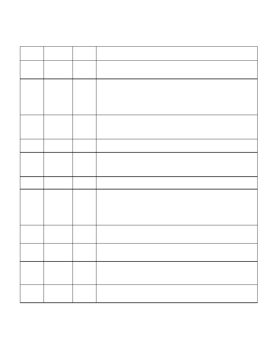
Table 1. Pin Descriptions
Pin
Numbers
Symbols
Type
Description
77
CLK
Input
Clock: CLK is driven by the system clock. All SDRAM input signals are sampled on
the positive edge of CLK. CLK also increments the internal burst counter and
controls the output registers.
79
CKE
Input
Clock enable: CKE activates (HIGH) and deactivates (LOW) the CLK signal.
Deactivating the clock provides PRECHARGE power-down, ACTIVE power-down
(row active in any bank), or CLOCK SUSPEND operation (burst/access in progress).
CKE is synchronous except after the device enters power-down where CKE becomes
asynchronous until after exiting the same mode. The input buffers, including CLK, are
disabled during power-down providing low standby power. CKE may be tied HIGH.
80
CS#
Input
Chip select: CS# enables (registered LOW) and disables (registered HIGH) the
command decoder. All commands are masked when CS# is registered HIGH. CS#
provides for external bank selection on systems with multiple banks. CS# is
considered part of the command code.
78, 76, 75 RAS#,CAS#,
WE#
Input
Input Command inputs: RAS#, CAS#, and WE# (along with CS#) define the command
being entered.
112, 16,
111, 59, 58
DQM(4:0)
Input
Input/output mask: DQM is an input mask signal for write accesses and an output
enable signal for read accesses. Input data is masked when DQM is sampled HIGH
during a WRITE cycle. The output buffers are placed in a High-Z state (two-clock
latency) when DQM is sampled HIGH during a READ cycle.
84 ,82
BA (1:0)
Input
Bank address inputs: BA0 and BA1 define to which bank the ACTIVE, READ, WRITE,
or PRECHARGE command is being applied.
81, 83, 86,
85, 87, 89,
91, 93, 95,
94, 92, 90,
88
A(12:0)
Input
Address inputs: A0–A12 are sampled during the ACTIVE command (row-address
A0–A12) and READ/WRITE command (column-address A0–A9, A11); with A10
defining auto precharge) to select one location out of the memory array in the respective
bank. A10 is sampled during a PRECHARGE command to determine whether all banks
are to be precharged (A10[HIGH]) or bank selected by (A10 [LOW]). The address inputs
also provide the opcode during a LOAD MODE REGISTER command.
42, 46, 50,
54, 56, 52,
48, 44
DQ[7.0](0)
Data I/O
Data input/output
43, 47, 51,
55, 57, 53,
49, 45
DQ[7:0](1)
Data I/O
Data input/output
127, 123,
119, 115,
113, 117,
121, 125
DQ[7:0](2)
Data I/O
Data input/output
32, 28, 24,
20, 18, 22,
26, 30
DQ[7:0](3)
Data I/O
Data input/output
相關(guān)PDF資料 |
PDF描述 |
|---|---|
| 5962F0253401VXC | 2.5 V FIXED POSITIVE REGULATOR, CDFP16 |
| L491333DIE2V | 3.3 V FIXED POSITIVE REGULATOR, UUC |
| 5962F9654403QXA | OTHER DECODER/DRIVER, CDFP16 |
| 5962F9657601QCX | AC SERIES, 4-BIT LOOK-AHEAD CARRY GENERATOR, TRUE OUTPUT, CDIP16 |
| 5962F9657701VXC | ACT SERIES, 4-BIT LOOK-AHEAD CARRY GENERATOR, TRUE OUTPUT, CDFP16 |
相關(guān)代理商/技術(shù)參數(shù) |
參數(shù)描述 |
|---|---|
| 5962D9563201VXC | 制造商:STMicroelectronics 功能描述:RS-432LINE DRIVERQUADFLAT16, GOLD - Bulk |
| 5962D9666301VXC | 制造商:STMicroelectronics 功能描述:RS-432LINE DRIVERQUADFLAT16, GOLD - Bulk |
| 5962F0052301QXC | 制造商:Intersil Corporation 功能描述: |
| 5962F0052301VXC | 制造商:Intersil Corporation 功能描述: |
| 5962F0151001VXC | 制造商:Intersil Corporation 功能描述:RAD SEU HARD QUAD COMPARATOR, CLASS V - Bulk |
發(fā)布緊急采購,3分鐘左右您將得到回復(fù)。