- 您現(xiàn)在的位置:買賣IC網(wǎng) > PDF目錄371556 > 2SK3592-01SJ (FUJI ELECTRIC CO LTD) N-CHANNEL SILICON POWER MOSFET PDF資料下載
參數(shù)資料
| 型號(hào): | 2SK3592-01SJ |
| 廠商: | FUJI ELECTRIC CO LTD |
| 元件分類: | JFETs |
| 英文描述: | N-CHANNEL SILICON POWER MOSFET |
| 中文描述: | 57 A, 150 V, 0.041 ohm, N-CHANNEL, Si, POWER, MOSFET |
| 文件頁(yè)數(shù): | 1/4頁(yè) |
| 文件大小: | 263K |
| 代理商: | 2SK3592-01SJ |
1
Item
Drain-source voltage
Symbol
V
DS
V
DSX *5
I
D
I
D(puls]
V
GS
I
AS *2
E
AS *1
dV
DS
/dt
*4
dV/dt
*3
P
D
Ta=25°C
Tc=25°C
T
ch
T
stg
Ratings
Unit
V
V
A
A
V
A
mJ
kV/μs
kV/μs
W
150
120
±57
±228
±30
Continuous drain current
Pulsed drain current
Gate-source voltage
Non-repetitive Avalanche current
Maximum Avalanche Energy
Maximum Drain-Source dV/dt
Peak Diode Recovery dV/dt
Max. power dissipation
57
272.5
20
5
1.67
270
+150
-55 to +150
Operating and storage
temperature range
*1 L=123μH, Vcc=48V, See to Avalanche Energy Graph *2 Tch =
Electrical characteristics (T
c
=25°C unless otherwise specified)
Thermalcharacteristics
2SK3592-01L,S,SJ
FUJI POWER MOSFET
Super FAP-G Series
N-CHANNEL SILICON POWER MOSFET
Features
High speed switching
Low on-resistance
No secondary breadown
Low driving power
Avalanche-proof
Applications
Switching regulators
UPS (Uninterruptible Power Supply)
DC-DC converters
Maximum ratings and characteristic
Absolute maximum ratings
(Tc=25°C unless otherwise specified)
Item
Symbol Test Conditions
R
th(ch-c)
channel to case
R
th(ch-a)
channel to ambient
Zero gate voltage drain current I
DSS
V
GS
=0V
V
GS
=0V
V
GS
=±30V
I
D
=20A V
GS
=10V
I
D
=20A V
DS
=25V
V
DS
=75V
V
GS
=0V
f=1MHz
V
CC
=48V I
D
=20A
V
GS
=10V
R
GS
=10
Min. Typ. Max. Units
150
3.0
V
V
μA
nA
m
S
pF
nC
A
V
μs
μC
ns
Min. Typ. Max. Units
Thermal resistance
0.463
75.0
°C/W
°C/W
Symbol
V
(BR)DSS
V
GS(th)
I
GSS
R
DS(on)
g
fs
C
iss
C
oss
C
rss
td
(on)
t
r
td
(off)
t
f
Q
G
Q
GS
Q
GD
I
AV
V
SD
t
rr
Q
rr
Item
Drain-source breakdown voltaget
Gate threshold voltage
Gate-source leakage current
Drain-source on-state resistance
Forward transcondutance
Input capacitance
Output capacitance
Reverse transfer capacitance
Turn-on time t
on
Turn-off time t
off
Total Gate Charge
Gate-Source Charge
Gate-Drain Charge
Avalanche capability
Diode forward on-voltage
Reverse recovery time
Reverse recovery charge
Test Conditions
I
D
= 250μA V
GS
=0V
I
D
= 250μA V
DS
=V
GS
=150V V
ch
=25°C
=120V V
ch
=125°C
V
DS
=0V
V
CC
=75V
I
D
=40A
V
GS
=10V
L=123μH T
ch
=25°C
I
F
=40A V
GS
=0V T
ch
=25°C
I
F
=40A V
GS
=0V
-di/dt=100A/μs T
ch
=25°C
°C
°C
5.0
25
250
100
41
10
31
26
13
1940
310
2910
465
24
20
26
50
20
52
15
18
36
30
39
75
30
78
22.5
27
57
1.10
0.14
0.77
1.65
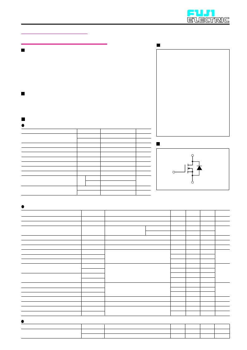
Outline Drawings
(mm)
Equivalent circuit schematic
Gate(G)
Source(S)
Drain(D)
*3 I
F
=
D
, -di/dt=50A/μs, Vcc=
DSS
, Tch=
*4 V
DS
<
www.fujielectric.co.jp/denshi/scd
*5 V
GS
=-30V
See to P4
200304
相關(guān)PDF資料 |
PDF描述 |
|---|---|
| 2SK3596-01SJ | N-CHANNEL SILICON POWER MOSFET |
| 2SK3597 | N-CHANNEL SILICON POWER MOSFET |
| 2SK3601-01 | N-CHANNEL SILICON POWER MOSFET |
| 2SK3606-01 | N-CHANNEL SILICON POWER MOSFET |
| 2SK3608 | N-CHANNEL SILICON POWER MOSFET |
相關(guān)代理商/技術(shù)參數(shù) |
參數(shù)描述 |
|---|---|
| 2SK3594-01 | 制造商:Fuji Electric 功能描述:MOSFET, Power;N-Ch;VDSS 200V;RDS(ON) 50 Milliohms;ID +/-45A;TO-220AB;PD 270W |
| 2SK3594-01SC | 制造商:Fuji Electric 功能描述: |
| 2SK3595-01MRSC | 制造商:Fuji Electric 功能描述: |
| 2SK3598-01SC | 制造商:Fuji Electric 功能描述: |
| 2SK3599-01MRSC-P | 制造商:Fuji Electric 功能描述: |
發(fā)布緊急采購(gòu),3分鐘左右您將得到回復(fù)。