- 您現(xiàn)在的位置:買賣IC網(wǎng) > PDF目錄371556 > 2SK3601-01 (FUJI ELECTRIC CO LTD) N-CHANNEL SILICON POWER MOSFET PDF資料下載
參數(shù)資料
| 型號: | 2SK3601-01 |
| 廠商: | FUJI ELECTRIC CO LTD |
| 元件分類: | JFETs |
| 英文描述: | N-CHANNEL SILICON POWER MOSFET |
| 中文描述: | 4.4 A, 100 V, 0.062 ohm, N-CHANNEL, Si, POWER, MOSFET |
| 封裝: | TFP, 4 PIN |
| 文件頁數(shù): | 1/4頁 |
| 文件大小: | 104K |
| 代理商: | 2SK3601-01 |
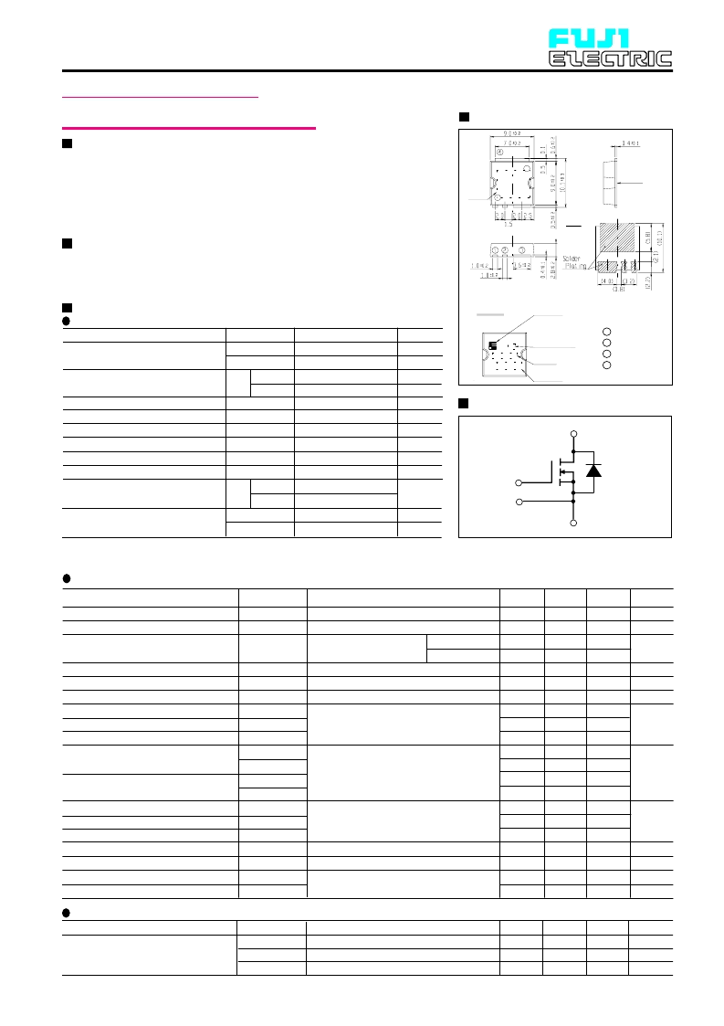
1
2 S1 : Source1
3 S2 : Source2
4 D : Drain
G
S1
FUJI POWER MOS FET
Fig.1
Fig.1
Note:1. Dimension shown in ( ) is
reference values.
Special
specification
for customer
Trademark
Lot No.
Type name
D
S2
MARKING
OUT VIEW
Outline Drawings
(mm)
DIMENSIONS ARE IN MILLIMETERS.
MARKING
CONNECTION
Item
Drain-source voltage
Symbol
V
DS
V
DSX *5
I
D
Tc=25°C
Ta=25°C
I
D(puls]
V
GS
I
AS *2
E
AS *1
dV
DS
/dt
*4
dV/dt
*3
P
D
Tc=25°C
Ta=25°C
T
ch
T
stg
Ratings
Unit
V
V
A
A
A
V
A
mJ
kV/μs
kV/μs
W
100
70
±20
±4.4
±80
±30
20
227
20
5
50
2.4 **
+150
-55 to +150
Continuous drain current
Pulsed drain current
Gate-source voltage
Non-repetitive Avalanche current
Maximum Avalanche Energy
Maximum Drain-Source dV/dt
Peak Diode Recovery dV/dt
Max. power dissipation
Operating and storage
temperature range
** Surface mounted on 1000mm
2
, t=1.6mm FR-4 PCB(Drain pad area : 500mm
2
)
Electrical characteristics (T
c
=25°C unless otherwise specified)
Thermalcharacteristics
2SK3601-01
FUJI POWER MOSFET
Super FAP-G Series
N-CHANNEL SILICON POWER MOSFET
Features
High speed switching
Low on-resistance
No secondary breadown
Low driving power
Avalanche-proof
Applications
Switching regulators
UPS (Uninterruptible Power Supply)
DC-DC converters
Maximum ratings and characteristic
Absolute maximum ratings
(Tc=25°C unless otherwise specified)
Item
Symbol Test Conditions
R
th(ch-c)
channel to case
R
th(ch-a)
channel to ambient
R
th(ch-a) **
channel to ambient
Zero gate voltage drain current I
DSS
DS
=100V V
GS
=0V
DS
=80V V
GS
=0V
V
GS
=±30V
I
D
=10A V
GS
=10V
I
D
=10A V
DS
=25V
V
DS
=75V
V
GS
=0V
f=1MHz
V
CC
=48V I
D
=10A
V
GS
=10V
R
GS
=10
Min. Typ. Max. Units
100
3.0
V
V
μA
nA
m
S
pF
nC
A
V
ns
μC
ns
Min. Typ. Max. Units
Thermal resistance
2.5
87.0
52.0
°C/W
°C/W
Symbol
V
(BR)DSS
V
GS(th)
I
GSS
R
DS(on)
g
fs
C
iss
C
oss
C
rss
td
(on)
t
r
td
(off)
t
f
Q
G
Q
GS
Q
GD
I
AV
V
SD
t
rr
Q
rr
Item
Drain-source breakdown voltaget
Gate threshold voltage
Gate-source leakage current
Drain-source on-state resistance
Forward transcondutance
Input capacitance
Output capacitance
Reverse transfer capacitance
Turn-on time t
on
Turn-off time t
off
Total Gate Charge
Gate-Source Charge
Gate-Drain Charge
Avalanche capability
Diode forward on-voltage
Reverse recovery time
Reverse recovery charge
Test Conditions
I
D
= 250μA V
GS
=0V
I
D
= 250μA V
DS
=V
GS
V
ch
=25°C
V
ch
=125°C
V
DS
=0V
V
CC
=50V
I
D
=20A
V
GS
=10V
L=100
μ
H T
ch
=25°C
I
F
=20A V
GS
=0V T
ch
=25°C
I
F
=20A V
GS
=0V
-di/dt=100A/μs T
ch
=25°C
°C
°C
5.0
25
250
100
62
10
47
12
730
190
12
12
6
1095
285
18
18
3.8
23
8.5
22
9
6
6
35
13
33
13.5
9
20
1.10
65
0.17
1.65
Equivalent circuit schematic
*3 I
F
=
D
, -di/dt=50A/μs, Vcc=
DSS
, Tch=
*1 L=681
μ
H, Vcc=48V *2 Tch=
*4 V
DS
<
*5 V
GS
=-30V
www.fujielectric.co.jp/denshi/scd
G : Gate
S2 : Source
D : Drain
S1 : Source
** Surface mounted on 1000mm
2
, t=1.6mm FR-4 PCB(Drain pad area : 500mm
2
)
相關(guān)PDF資料 |
PDF描述 |
|---|---|
| 2SK3606-01 | N-CHANNEL SILICON POWER MOSFET |
| 2SK3608 | N-CHANNEL SILICON POWER MOSFET |
| 2SK3608-01L | N-CHANNEL SILICON POWER MOSFET |
| 2SK3608-S | N-CHANNEL SILICON POWER MOSFET |
| 2SK3608-SJ | N-CHANNEL SILICON POWER MOSFET |
相關(guān)代理商/技術(shù)參數(shù) |
參數(shù)描述 |
|---|---|
| 2SK3603-01MRSC | 制造商:Fuji Electric 功能描述: |
| 2SK3604-01LSC | 制造商:Fuji Electric 功能描述: |
| 2SK3606-01 | 制造商:Fuji Electric 功能描述:MOSFET, Power;N-Ch;VDSS 200V;RDS(ON) 131 Milliohms;ID +/-18A;TO-220AB;PD 105W |
| 2SK3606-01SC | 制造商:Fuji Electric 功能描述: |
| 2SK3607 | 制造商:Panasonic Industrial Company 功能描述:TRANSISTOR |
發(fā)布緊急采購,3分鐘左右您將得到回復(fù)。