- 您現(xiàn)在的位置:買賣IC網(wǎng) > PDF目錄384068 > μPD98402A (NEC Corp.) Ultraframer DS3/E3/DS2/E2/DS1/E1/DS0 PDF資料下載
參數(shù)資料
| 型號(hào): | μPD98402A |
| 廠商: | NEC Corp. |
| 元件分類: | 通信及網(wǎng)絡(luò) |
| 英文描述: | Ultraframer DS3/E3/DS2/E2/DS1/E1/DS0 |
| 中文描述: | Ultraframer DS3/E3/DS2/E2/DS1/E1/DS0 |
| 文件頁(yè)數(shù): | 11/26頁(yè) |
| 文件大小: | 178K |
| 代理商: | ΜPD98402A |
第1頁(yè)第2頁(yè)第3頁(yè)第4頁(yè)第5頁(yè)第6頁(yè)第7頁(yè)第8頁(yè)第9頁(yè)第10頁(yè)當(dāng)前第11頁(yè)第12頁(yè)第13頁(yè)第14頁(yè)第15頁(yè)第16頁(yè)第17頁(yè)第18頁(yè)第19頁(yè)第20頁(yè)第21頁(yè)第22頁(yè)第23頁(yè)第24頁(yè)第25頁(yè)第26頁(yè)
μ
PD98402A
11
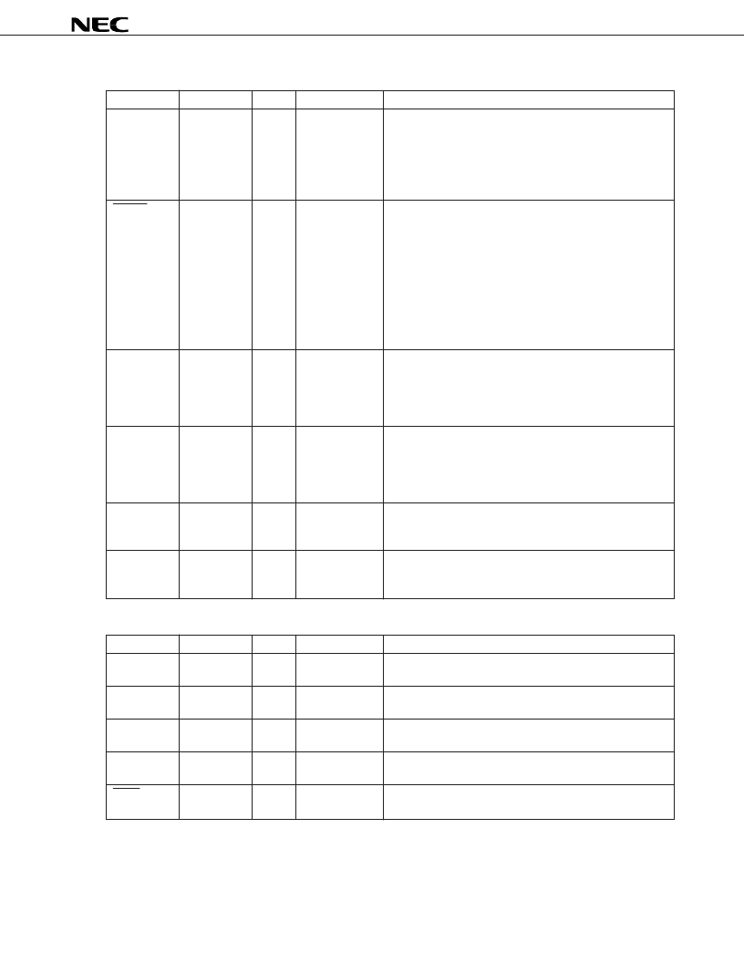
Control
Symbol
Pin No.
I/O
I/O Level
Function
TFSS
29
I
TTL
This is the transmit frame setting signal input pin.
It allows synchronization timing of transmit frame output to be
set. The
μ
PD98402A samples this input signal by the internal
transmit system clock (TCL).
Initial output of the transmit frame is restarted 9 clocks into
TCL clock cycle after a high level is latched at TCL rise.
RESET
103
I
TTL
This is the system reset signal input pin.
It initializes the
μ
PD98402A. It is necessary to input a reset
signal with a pulse width of 2 cycles or more of the clock that
has the longest cycle among the following clocks input to the
μ
PD98402A.
ATM layer
:
TCLK, RCLK clock cycles
PMD layer
:
1/8 cycle of TFKT/TFKC, RCIC/RCIT clocks,
TFC, RPC clock cycles
Immediately after a reset, no read/write is possible to registers
during 5 clocks of the TCL clock (19.44 MHz).
TCL
32
O
CMOS
This pin is used to output an internal transmit system clock.
The
μ
PD98402A outputs as the internal transmit system clock,
the TFKT/TFKC input clock (155.52 MHz) scaled by 8 in serial
interface mode, and the TFC input clock (19.44 MHz) in
parallel interface mode.
RCL
85
O
CMOS
This pin is used to output an internal receive system clock.
The
μ
PD98402A outputs as the internal receive system clock,
the RCIC/RCIT input clock (155.52 MHz) scaled by 8 in serial
interface mode, and the RFC input clock (19.44 MHz) in
parallel interface mode.
TxFP
31
O
CMOS
This is a frame pulse signal on the transmitting side. It
outputs pulses synchronous with the transmit frame start. To
be inactive after reset.
RxFP
30
O
CMOS
This is a frame pulse signal on the receiving side. It outputs
pulses synchronous with the receive frame start. To be
inactive after reset.
JTAG boundary scan pins (This function can be supported at the customer’s request.)
Symbol
Pin No.
I/O
I/O Level
Function
TJI
4
I
TTL
This is a pin for JTAG boundary scan.
Pull it up or ground it in normal operation.
TDO
3
O
CMOS
This is a pin for JTAG boundary scan.
Leave it open in normal operation.
TCK
2
I
TTL
This is a pin for JTAG boundary scan.
Pull it up or ground it in normal operation.
TMS
5
I
TTL
This is a pin for JTAG boundary scan.
Pull it up or ground it in normal operation.
TRST
6
I
TTL
This is a pin for JTAG boundary scan.
Ground it in normal operation.
相關(guān)PDF資料 |
PDF描述 |
|---|---|
| μPD98402 | Ultraframer DS3/E3/DS2/E2/DS1/E1/DS0 |
| μPD98404 | High-performance ATM controller(高性能異步傳輸模式控制器) |
| μPD98405 | 155M ATM Integrated SAR Controller(155M ATM SAR集成控制器) |
| μPD98408 | ATM Physical Interface(ATM 物理接口) |
| μPD98411 | Ultraframer DS3/E3/DS2/E2/DS1/E1/DS0 |
相關(guān)代理商/技術(shù)參數(shù) |
參數(shù)描述 |
|---|---|
| PD98CNT30QMU | 制造商:Carlo Gavazzi 功能描述:PHOTO TS PL 30M AC/DC NO+NC |
| PD9909-59 | 制造商:Philco/Philips 功能描述: |
| PD9930-51 | 制造商:Philco/Philips 功能描述: |
| PD9933-59 | 制造商:Philco/Philips 功能描述: |
| PD9941-59 | 制造商:Philco/Philips 功能描述: |
發(fā)布緊急采購(gòu),3分鐘左右您將得到回復(fù)。